XC2S50-5TQG144I FPGA: Features, Specifications, Applications and Programming Guide
The XC2S50-5TQG144I is a flexible and powerful FPGA (Field Programmable Gate Array) from AMD Xilinx's Spartan-II family. It is designed for digital projects that need customization, speed, and reliability. This guide explains the features, specifications, programming process, and uses of this FPGA to help you understand how to make the most of it.Catalog
XC2S50-5TQG144I Overview
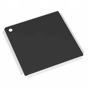
The XC2S50-5TQG144I is a Spartan-II FPGA from AMD Xilinx, designed for digital projects that need flexibility and performance. It has 50,000 system gates and 1,728 logic cells, allowing it to handle complex tasks. The chip includes 384 Configurable Logic Blocks (CLBs) and 32,768 RAM bits, giving it good memory and processing power. With 92 input/output (I/O) pins, it can easily connect to other components. It comes in a 144-pin Thin Quad Flat Pack (TQFP), which is compact and easy to use. The FPGA runs on 2.5V (with a safe range of 2.375V to 2.625V) and works well in temperatures between -40°C and +100°C. This Spartan-II FPGA is made with 0.18-micron technology, making it efficient and reliable. It is programmable, meaning you can update its functions as needed.
For a cost-effective, high-performance solution, placing a bulk order with us is the optimal choice, ensuring superior quality.
XC2S50-5TQG144I CAD Models
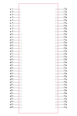
XC2S50-5TQG144I Symbol
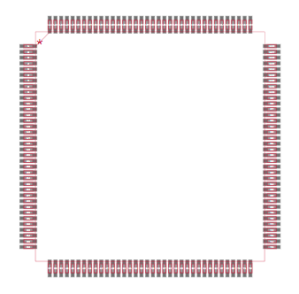
XC2S50-5TQG144I Footprint
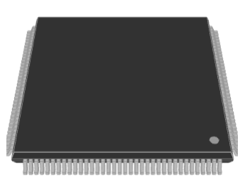
XC2S50-5TQG144I 3D Model
XC2S50-5TQG144I Features
• System Gates: The XC2S50-5TQG144I FPGA offers approximately 50,000 system gates. This allows it to support complex digital designs and applications requiring a substantial amount of logic processing capabilities.
• Logic Cells: This device includes 1,728 logic cells, which facilitate the implementation of intricate logic configurations and creating various digital functionalities within the FPGA.
• Configurable Logic Blocks (CLBs): It features 384 Configurable Logic Blocks (CLBs), providing the foundation for the FPGA's logic. These blocks can be programmed and reconfigured to meet specific design requirements, enhancing the overall versatility of the device.
• RAM: The FPGA is equipped with 32,768 bits of internal RAM, offering efficient data storage and retrieval capabilities for tasks involving data manipulation and temporary data storage.
• I/O Pins: With 92 I/O pins, the XC2S50-5TQG144I ensures ample external connectivity, allowing it to interface with other devices and components in a system for comprehensive system integration.
• Operating Voltage: The device operates at a nominal voltage of 2.5V, with an acceptable range from 2.375V to 2.625V. This voltage range helps ensure stable operation and reliable performance under various electrical conditions.
• Temperature Range: The XC2S50-5TQG144I is designed to operate effectively in a wide temperature range, from -40°C to +100°C, making it suitable for deployment in environments with challenging thermal conditions.
XC2S50-5TQG144I Block Diagram
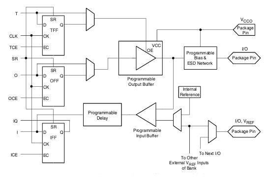
The diagram shows how signals move in and out of the XC2S50-5TQG144I FPGA. It explains how the chip handles input and output signals to communicate with other components. On the output side, signals come from inside the FPGA and go through storage units called flip-flops. These flip-flops hold data and make sure signals change at the right time. The signals then pass through a programmable output buffer, which adjusts how strong the signal is and controls how fast it changes. There is also a switch (OE control) that decides if the output should be active or stay off. A protection circuit prevents damage from static electricity before the signal reaches the I/O pins, which connect to other devices. On the input side, signals from outside enter through the programmable input buffer, which processes them before sending them inside the FPGA. A programmable delay unit helps adjust signal timing so everything stays in sync. The FPGA can also use an internal reference voltage (VREF) to match different voltage levels, making it easier to work with different types of circuits. Some I/O pins share this voltage reference to keep signals stable. This design helps the FPGA manage signals efficiently, ensuring proper timing, protection, and compatibility with different electronic components.
XC2S50-5TQG144I Specifications
|
Type |
Parameter |
|
Manufacturer |
AMD Xilinx |
|
Series |
Spartan®-II |
|
Packaging |
Tray |
|
Part Status |
Obsolete |
|
Number of LABs/CLBs |
384 |
|
Number of Logic Elements/Cells |
1728 |
|
Total RAM Bits |
32,768 |
|
Number of I/O |
92 |
|
Number of Gates |
50,000 |
|
Voltage - Supply |
2.375V ~ 2.625V |
|
Mounting Type |
Surface Mount |
|
Operating Temperature |
-40°C ~ 100°C (TJ) |
|
Package / Case |
144-LQFP |
|
Supplier Device Package |
144-TQFP (20x20) |
|
Base Product Number |
XC2S50 |
XC2S50-5TQG144I Applications
Embedded Systems
In embedded systems, the XC2S50-5TQG144I provides the necessary logic for microcontroller-based applications. It is extensively used in automotive electronics, portable devices, and small-scale robotics to enhance functionality and responsiveness.
Signal Processing
The FPGA excels in signal processing tasks, where its ability to perform parallel processing is required. It is ideal for audio and video processing, telecommunications, and data analysis, providing the horsepower to handle complex algorithms and high-speed data streams.
Industrial Control Systems
Industrial control systems benefit from this FPGA's robustness and programmability, making it suitable for applications such as process control, machine automation, and system monitoring. Its reliability ensures consistent performance in environments requiring precision and operational stability.
Communication Systems
In communication systems, the XC2S50-5TQG144I helps manage data transmission and reception, supporting activities such as signal modulation and demodulation, protocol conversion, and network routing. Its adaptability is key in evolving telecommunications infrastructures and emerging wireless technologies.
Prototyping and Development
The FPGA is also used extensively for prototyping digital circuits. Many utilize it to test and refine their ideas before final production, especially in complex ASIC and custom chip design projects. This capability reduces development time and costs, accelerating the path from concept to market.
XC2S50-5TQG144I Similar Parts
XC2S50-5TQG144I Advantages
Cost-Effectiveness
The XC2S50-5TQG144I stands out for its affordability, delivering more features per dollar than many competing FPGAs. This cost-effectiveness is achieved through advanced process technology and an efficient architecture, enabling broader deployment in cost-sensitive markets.
High-Performance I/O and Packaging
This FPGA supports a wide range of I/O standards and is available in various cost-effective packaging options. These features ensure that the device can be integrated into multiple applications without sacrificing performance, making it ideal for both high-end and volume-driven markets where interface versatility and physical constraints are factors.
System-Level Features
Equipped with advanced memory management features such as distributed RAM and configurable block RAM, the XC2S50-5TQG144I enhances data handling efficiency. These features facilitate complex data storage and processing tasks, boosting the system's overall performance and scalability.
Reprogrammability
The reprogrammability of the XC2S50-5TQG144I allows unlimited modifications to its configuration, which is beneficial during the development phase. This flexibility enables to refine designs through iterative updates without additional hardware costs, fostering innovation and reducing time to final product.
XC2S50-5TQG144I Programming Steps
Programming the XC2S50-5TQG144I FPGA from AMD Xilinx's Spartan-II series involves a structured series of steps designed to efficiently translate a digital design into a functional FPGA configuration. Here’s an integrated and detailed guide to help you through the programming process:
1. Design Entry
Begin with the design entry phase, where you create your digital logic using a Hardware Description Language (HDL), such as VHDL or Verilog. This initial step involves detailing the functionality and logic that you want to implement in the FPGA. It is required that your design is precise and accurately represents the intended operations to ensure successful synthesis and implementation.
2. Synthesis
In the synthesis step, utilize a synthesis tool to convert your HDL code into a netlist. A netlist is a breakdown of your design into a format that includes various interconnected logical elements such as gates and flip-flops. This process translates your theoretical design into a practical blueprint that the FPGA can understand and implement.
3. Implementation
Implementation involves several sub-steps: mapping, placing, and routing. Mapping assigns the elements of your netlist to specific logic blocks within the FPGA. Placing determines the physical locations of these blocks on the FPGA chip to optimize performance and resource utilization. Routing connects these blocks through the FPGA’s programmable interconnect resources. This phase ensures that the design meets all physical and performance constraints.
4. Constraint Definition
During the design process, defining constraints is needed. Constraints guide the implementation tools by specifying requirements such as timing (how fast the FPGA should operate), and pin assignments (which pins on the FPGA will connect to different parts of your hardware). These are articulated in a User Constraints File (UCF), which helps in fine-tuning the design to meet specific operational standards.
5. Bitstream Generation
Once your design successfully passes through the implementation phase, the next step is to generate a bitstream file. This file contains all the configuration data needed by the FPGA to execute the design. The bitstream is the final output of the programming process, representing the complete, programmed state of the FPGA.
6. Device Programming
The final step is to load the bitstream into the XC2S50-5TQG144I FPGA, which can be done using various configuration modes depending on your setup. In Master Serial Mode, the FPGA autonomously reads the configuration data from an attached serial PROM (Programmable Read-Only Memory). Slave Serial Mode allows an external master device, such as a microcontroller, to feed the FPGA configuration data serially. Slave Parallel Mode enables high-speed programming by supplying configuration data in parallel from an external master device. Lastly, Boundary Scan (JTAG) Mode utilizes the JTAG interface for both programming and testing, making it useful during development for iterative debugging and verification.
XC2S50-5TQG144I Packaging Dimensions
The XC2S50-5TQG144I is a Field Programmable Gate Array (FPGA) from Xilinx's Spartan-II family, housed in a 144-pin Thin Quad Flat Pack (TQFP) package. This package measures 20 mm x 20 mm.
XC2S50-5TQG144I Manufacturer
The XC2S50-5TQG144I is an FPGA from the Spartan-II family, manufactured by AMD Xilinx. Xilinx, now part of AMD, is a leading semiconductor company specializing in FPGAs, adaptive SoCs, and other programmable logic devices. The XC2S50-5TQG144I was originally developed under the Xilinx Spartan-II series, offering 50,000 system gates and 1,728 logic cells, designed for high-performance yet cost-effective applications. With Xilinx's acquisition by AMD, the company continues to support legacy products like the Spartan-II series while advancing newer FPGA architectures. However, the XC2S50-5TQG144I is an older-generation FPGA and may face eventual obsolescence as AMD Xilinx shifts focus to more advanced FPGA families.
Conclusion
The XC2S50-5TQG144I FPGA is a cost-effective and reprogrammable chip that offers great performance and flexibility. It is widely used in embedded systems, industrial machines, and communication networks because of its high-speed processing and strong connectivity options. With its ability to be programmed and updated, this FPGA helps test and develop new ideas before final production. Although newer FPGAs are available, this model remains a solid choice for projects that need a reliable and affordable FPGA solution. This guide provides a clear and simple overview of the FPGA’s features, uses, and programming process, making it a valuable resource for everyone.
About us
ALLELCO LIMITED
Read more
Quick inquiry
Please send an inquiry, we will respond immediately.
Frequently Asked Questions [FAQ]
1. Can I use the XC2S50-5TQG144I for high-speed applications?
The XC2S50-5TQG144I supports speeds up to 200 MHz, making it suitable for most embedded and industrial applications. However, if your project requires high-speed interfaces like PCIe or DDR memory, you may need a more advanced FPGA like the Spartan-6 or Artix-7 series.
2. How does the XC2S50-5TQG144I compare to the newer Spartan-3 or Spartan-6 FPGAs?
While newer FPGAs like Spartan-3 or Spartan-6 offer enhanced performance, higher logic density, and additional features, the XC2S50-5TQG144I remains a preferred choice for cost-sensitive projects with moderate complexity. If you require legacy compatibility or a stable supply chain, the XC2S50-5TQG144I is a great option.
3. What programming tools are compatible with the XC2S50-5TQG144I FPGA?
The XC2S50-5TQG144I is programmed using Xilinx ISE (Integrated Software Environment). While newer Xilinx tools such as Vivado do not support the Spartan-II family, ISE provides all the necessary design, synthesis, and programming functionalities for this FPGA.
4. Can I migrate an existing Spartan-II design to a newer FPGA?
Yes, but it requires modifications. The newer Spartan-3 and Spartan-6 families use different architecture, voltage levels, and configuration methods. If you are considering migration, we can assist in selecting suitable alternatives and minimizing design changes.
5. Does the XC2S50-5TQG144I support JTAG programming?
A: Yes, the FPGA supports JTAG (IEEE 1149.1) boundary scan programming, which allows easy debugging and configuration using a standard JTAG interface. This is useful for both initial programming and reconfiguration without external memory.
XC4013XL-3PQ240C FPGA: Alternatives, Specifications, Applications, and Datasheet
on March 18th
RF Power Amplifiers: How They Work, Which Type Is More Efficient
on March 18th
Popular Posts
-

Complex Instruction Set Computers: How They Changed Computing?
on April 18th 147760
-

USB-C Pinout and Features
on April 18th 111974
-

Using Xilinx Unified Simulation Primitives: A Comprehensive Guide to FPGA Design and Simulation
on April 18th 111351
-

Power Supply Voltages in Electronics: Meaning of VCC, VDD, VEE, VSS, and GND
on April 18th 83742
-

RJ45 Connector Guide: Pinout, Wiring, Cable Types, and Uses
on January 1th 79527
-

The Ultimate Guide to Wire Color Codes in Modern Electrical Systems
The way our electrical systems use colors isn’t just for looks. Each wire color now indicates a specific function, making it easier to identify and handle electrical components correctly during ins...on January 1th 66937
-

Purge Valve Guide: Function, Symptoms, Testing, and Replacement for Optimal Engine Performance
The purge valve is a key part of a car’s system that helps keep the air clean by managing fuel vapors before they can escape into the atmosphere. This not only helps the environment by reducing pol...on January 1th 63086
-

Quality (Q) Factor: Equations and Applications
The quality factor, or 'Q', is important when checking how well inductors and resonators work in electronic systems that use radio frequencies (RF). 'Q' measures how well a circuit minimizes energy...on January 1th 63025
-

Achieving Peak Performance with the Maximum Power Transfer Theorem
The Maximum Power Transfer Theorem explains how energy from a source, such as a battery or generator, flows to a connected load. It shows the exact condition where the load receives the most power....on January 1th 54092
-

A23 Battery Specifications and Compatibility
The A23 battery is a small, cylinder-shaped battery with high voltage. Also called 23A, 23AE, or MN21, it runs at 12 volts and much higher than AA or AAA batteries. Its special design make...on January 1th 52167
HOT Part Number
-

JANTX1N751A-1
MACOM Technology Solutions
DIODE ZENER 5.1V 500MW DO35
74ALVCH16245ZQLR
Texas Instruments
IC TXRX NON-INVERT 3.6V 56BGA
NTE5252AK
NTE Electronics, Inc
DIODE ZENER 10V 50W DO5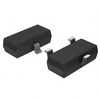
BAV170_R1_00001
Panjit International Inc.
SOT-23, SWITCHING
OPA657U
Texas Instruments
IC VOLTAGE FEEDBACK 1 CIRC 8SOIC
MIXA30WB1200TED
IXYS
IGBT MODULE 1200V 43A 150W E2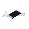
WSLP1206R0200FEA
Vishay Dale
RES 0.02 OHM 1% 1W 1206
502237-0517
Molex
USB Mini-B Receptacle, Vertical,
MB89935DPFV-GS-109-ERE1
Infineon Technologies
IC MCU 8BIT 16KB MROM 30SSOP
C1812C334K1RAC7800
KEMET
CAP CER 0.33UF 100V X7R 1812
ADL5565ACPZ-R7
Analog Devices Inc.
IC OPAMP RF/IF DIFF 1CIR 16LFCSP
KSP94BU
onsemi
TRANS PNP 400V 0.3A TO92-3
LTC2619IGN#PBF
Analog Devices Inc.
IC DAC 14BIT V-OUT 16SSOP
TLV1117-25CKVURG3
Texas Instruments
IC REG LINEAR 2.5V 800MA TO252-3
IRF7413PBF
International Rectifier
MOSFET N-CH 30V 13A 8SO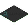
MPC8572EVTAVND
Freescale Semiconductor
MPU, 32-BIT, 1500MHZ, PBGA1023
GRM1886T1H7R2DD01D
Murata Electronics
CAP CER 7.2PF 50V T2H 0603
FAN23SV06PAMPX
onsemi
IC REG BUCK ADJUSTABLE 6A 34PQFN -

9EPRS525AGLFT
Renesas Electronics America Inc
IC EMBEDDED PC MAIN CLK 56TSSOP
MHQ0402PSA3N3BT000
TDK Corporation
FIXED IND 3.3NH 250MA 650MOHM SM
XC7VX415T-2FFG1157I
AMD
IC FPGA 600 I/O 1157FCBGA
1N5233B
onsemi
DIODE ZENER 6V 500MW DO35
IRFP4321PBF
Infineon Technologies
MOSFET N-CH 150V 78A TO247AC
GRM155R71C224KA12D
Murata Electronics
CAP CER 0.22UF 16V X7R 0402
TPS65140PWPRG4
Texas Instruments
IC LCD SUPPLY TFT QUAD 24HTSSOP
MA12RTR
APEM Inc.
SWITCH SLIDE SPDT 300MA 4V
TSV6191ILT
STMicroelectronics
IC OPAMP GP 1 CIRCUIT SOT23-5
06035AR47CAT2A
KYOCERA AVX
CAP CER 0.47PF 50V NP0 0603
AD7858LARSZ
Analog Devices Inc.
IC ADC 12BIT SAR 24SSOP
0603ZC224KA12A
KYOCERA AVX
CAP CER 0.22UF 10V X7R 0603
CD4528BCN
onsemi
IC MULTIVIBRATOR 65NS 16DIP
1N4754A-TAP
Vishay General Semiconductor - Diodes Division
DIODE ZENER 39V 1.3W DO41
EP2C50F672C7N
Intel
IC FPGA 450 I/O 672FBGA
MTFC16GAKAEJP-5M AIT
Micron Technology Inc.
IC FLASH 128GBIT MMC 153VFBGA
OPA2337PA
Texas Instruments
IC CMOS 2 CIRCUIT 8DIP
12TQ045
SMC Diode Solutions
DIODE SCHOTTKY 45V 15A TO220AC -
AT49BV040B-JU
Microchip Technology
IC FLASH 4MBIT PARALLEL 32PLCC
XCS20-3TQ144I
AMD
IC FPGA 113 I/O 144TQFP
DS4156P+
Analog Devices Inc./Maxim Integrated
IC OSC CLOCK 156.25MHZ 10-LCCC
LTC1709EG-7#TRPBF
Analog Devices Inc.
IC REG CTRLR BUCK 36SSOP
IHLP3232DZER3R3M01
Vishay Dale
FIXED IND 3.3UH 9.2A 17.7MOHM SM
ADP150AUJZ-3.3-R7
Analog Devices Inc.
IC REG LINEAR 3.3V 150MA TSOT5
24VL014T/MNY
Microchip Technology
IC EEPROM 1KBIT I2C 400KHZ 8TDFN
CY62137CV30LL-55BAI
Cypress Semiconductor Corp
IC SRAM 2MBIT PARALLEL 48FBGA
06031A100CAT2A
AVX Corporation
CAP CER 10PF 100V C0G/NP0 0603
XCS20XL-4VQG100C
AMD
IC FPGA 77 I/O 100VQFP
IS43R16320F-5TL
ISSI, Integrated Silicon Solution Inc
512M, 2.5V, DDR 32Mx16, 200MHz,
C2012X7T2W223K125AE
TDK Corporation
CAP CER 0.022UF 450V X7T 0805
CGA5L1X7R1V685M160AC
TDK Corporation
CAP CER 6.8UF 35V X7R 1206
744031330
Würth Elektronik
FIXED IND 33UH 420MA 660MOHM SMD
1N2055
Solid State Inc.
DIODE GEN PURP 100V 275A DO9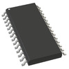
LT1943EFE#TRPBF
Analog Devices Inc.
IC REG CONV TFT LCD 4OUT 28TSSOP
STTH2R02U
STMicroelectronics
DIODE GEN PURP 200V 2A SMB
1N3326RB
Microchip Technology
DIODE ZENER 36V 50W DO5