XC3S200-4TQG144I FPGA: Features, Pinout, Programming, and Applications
This guide is all about the XC3S200-4TQG144I, which is known for offering strong performance at a low cost. This chip has many useful features like thousands of logic cells, built-in memory, special math units, and plenty of input/output pins. In this article, you’ll learn what this chip does, how it works, where you can use it, and how to program it for your own projects.Catalog
XC3S200-4TQG144I Overview
The XC3S200-4TQG144I is part of AMD Xilinx's Spartan-3 FPGA family, tailored for cost-sensitive applications that demand high performance. This model features 200,000 system gates and utilizes 4,320 logic cells, enabling robust processing capabilities in a compact form factor. The device boasts substantial internal resources, including 480 Configurable Logic Blocks (CLBs), 216 Kbits of block RAM for data storage, and 12 dedicated 18x18 multipliers for enhanced arithmetic operations. It supports up to 97 user I/O pins, allowing versatile connectivity options. Clock management is efficiently handled by four Digital Clock Managers (DCMs), facilitating precise timing and control within high-speed digital environments. The XC3S200-4TQG144I operates on a 1.2V core voltage, with an allowable range of 1.14V to 1.26V, and it is designed to perform reliably in industrial settings with a temperature range of -40°C to +100°C. The maximum achievable clock frequency for this FPGA is up to 630 MHz, ensuring rapid data processing and responsiveness in applications.
If you're running a business and need a steady supply of reliable, high-performance FPGAs, the XC3S200-4TQG144I is a smart choice. Placing your bulk order with us boosts your system's performance, and we're here to support you every step of the way.
XC3S200-4TQG144I CAD Models
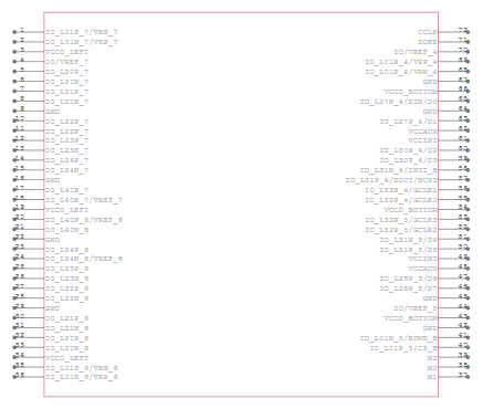
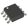
XC3S200-4TQG144I Symbol
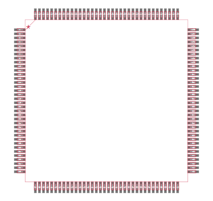
XC3S200-4TQG144I Footprint

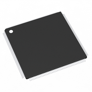
XC3S200-4TQG144I 3D Model
XC3S200-4TQG144I Features
• Logic Capacity: The XC3S200-4TQG144I offers a substantial logic capacity with 200,000 system gates and 4,320 logic cells. This allows you to implement complex digital circuits and systems within a single chip, making it ideal for a variety of applications that require computational power and flexibility.
• Configurable Logic Blocks (CLBs): This FPGA is equipped with 480 Configurable Logic Blocks, which are the main logic resource for implementing user-defined logic functions. Each CLB can be programmed to perform a wide range of logical operations, providing the flexibility needed to optimize performance and resource utilization.
• Memory Resources: It includes 216 Kbits of block RAM and up to 520 Kbits of distributed RAM. This on-chip memory is important for applications that require fast and efficient data storage and retrieval, supporting everything from buffering and data caching to complex state machines.
• Dedicated Multipliers: Featuring 12 dedicated 18x18 multipliers, the XC3S200-4TQG144I excels in applications requiring intensive mathematical computations such as digital signal processing, video processing, and control systems.
• Digital Clock Managers (DCMs): The FPGA incorporates four Digital Clock Managers that provide advanced clocking capabilities. DCMs enhance the flexibility and accuracy of clock management, enabling frequency synthesis, phase shifting, and jitter reduction, which are needed for high-speed digital communications and precise timing applications.
• I/O Capabilities: With 97 user I/O pins, the FPGA supports a variety of single-ended and differential I/O standards, including LVDS and RSDS. This extensive I/O capability enables easy integration with a wide range of peripherals and systems, ensuring versatility in deployment across different hardware environments.
• Operating Conditions: Designed to perform reliably in industrial environments, the XC3S200-4TQG144I operates within a temperature range of –40°C to +100°C. This robust temperature tolerance makes it suitable for deployment in harsh operational conditions.
• Power Supply: It operates on a core voltage of 1.2V, with an allowable range from 1.14V to 1.26V. This low-power operation is great for applications that are sensitive to power consumption, helping to reduce overall system energy requirements.
• Compliance: The XC3S200-4TQG144I meets RoHS and REACH standards, ensuring compliance with current environmental and safety regulations. This compliance supports companies in maintaining sustainable and responsible manufacturing practices.
XC3S200-4TQG144I Pinout Diagram
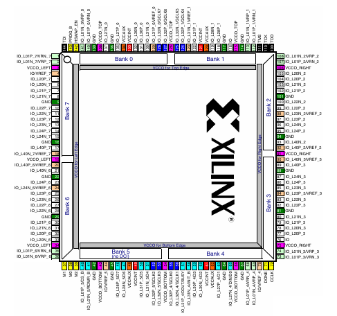
The pinout diagram for the XC3S200-4TQG144I FPGA from the Xilinx Spartan-3 family shows the physical pin configuration and signal assignments for the 144-pin Thin Quad Flat Pack (TQFP) package. The diagram is laid out in a square format representing the top view of the chip, with pin numbers labeled around the perimeter. Each side corresponds to a specific bank (Bank 0 to Bank 7), which groups I/O pins with shared voltage references.
Each colored box represents a signal type or voltage function such as I/O signals, power supply pins (VCCINT, VCCO), ground (GND), configuration pins (like INIT_B or DONE), and special function pins (such as clock inputs or JTAG). The IO_L naming convention identifies differential I/O pairs (like IO_LxxN_Pxxx or IO_LxxP_Pxxx), useful in high-speed data interfaces. Some pins are reserved for configuration, programming, or dedicated clock functions, which are important for device setup and operation.
XC3S200-4TQG144I Block Diagram
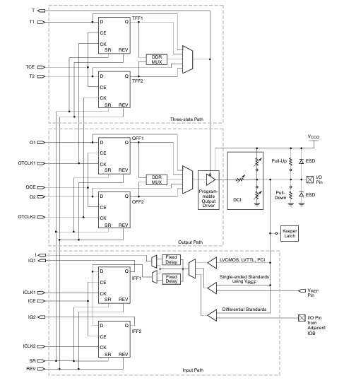
The block diagram of the XC3S200-4TQG144I, a Spartan-3 FPGA from AMD (formerly Xilinx), illustrates the internal architecture of an I/O Block (IOB), detailing how signals flow between the FPGA fabric and the external pins. This diagram represents the programmable logic and configurable paths that control input, output, and tristate behavior for each I/O pin.
At the top, the Three-state Path handles output enable signals. Flip-flops (TFF1, TFF2) receive control signals (T1, T2) and timing control signals (TCE, TCK) to determine whether the output drivers are active or in a high-impedance state. A multiplexer selects between different sources based on programmable configuration.
In the middle, the Output Path includes flip-flops (OFF1, OFF2) that store output data signals (O1, O2) synchronized with output clocks (OTCLK1, OTCLK2). A multiplexer and optional DDR (Double Data Rate) logic allow data to be driven on both rising and falling clock edges. The output driver connects to various logic for DCI (Digitally Controlled Impedance) and supports pull-up/pull-down resistors, ESD protection, and keeper latches to maintain line state when undriven.
At the bottom, the Input Path shows how input signals (IQ1, IQ2) are latched into flip-flops (IFF1, IFF2) using input clocks (ICLK1, ICLK2). Optional delays are programmable to fine-tune timing. Inputs support multiple I/O standards including LVCMOS, LVTTL, and differential signals using VREF and adjacent pins.
XC3S200-4TQG144I Specifications
|
Type |
Parameter |
|
Manufacturer |
AMD |
|
Series |
Spartan®-3 |
|
Packaging |
Tray |
|
Part Status |
Obsolete |
|
Number of LABs/CLBs |
480 |
|
Number of Logic Elements/Cells |
4320 |
|
Total RAM Bits |
221184 |
|
Number of I/O |
97 |
|
Number of Gates |
200000 |
|
Voltage - Supply |
1.14V ~ 1.26V |
|
Mounting Type |
Surface Mount |
|
Operating Temperature |
-40°C ~ 100°C (TJ) |
|
Package / Case |
144-LQFP |
|
Supplier Device Package |
144-TQFP (20x20) |
|
Base Product Number |
XC3S200 |
XC3S200-4TQG144I Applications
Digital Signal Processing (DSP)
The XC3S200-4TQG144I excels in DSP applications due to its dedicated multipliers and substantial block RAM. This makes it ideal for tasks requiring intensive mathematical computations such as audio and video processing, where it can handle operations like filtering, modulation, and compression efficiently.
Embedded Systems
This FPGA supports soft-core processors like MicroBlaze and PicoBlaze, which allow for the development of complex embedded systems. It's used in custom control systems, smart devices, and user interfaces where tailored functionality is important.
Industrial Automation
With its robust I/O capabilities and ability to operate reliably in extreme temperatures, the XC3S200-4TQG144I is perfectly suited for industrial automation. It manages motor control, sensor interfacing, and monitoring systems, helping to optimize and automate complex industrial processes.
Automotive Electronics
In automotive electronics, the FPGA enables functionalities ranging from infotainment systems to complex dashboard controls and advanced driver-assistance systems (ADAS). Its high reliability and adaptability make it a go-to choice for automotive manufacturers.
Communication Systems
The XC3S200-4TQG144I is instrumental in communication infrastructure, such as routers, switches, and wireless base stations. Its high-speed processing capabilities ensure efficient data handling and communication across networks.
Educational and Prototyping Platforms
Due to its cost-effectiveness and versatility, the FPGA is widely used in educational settings for teaching digital design and FPGA technology. It is also favored in prototyping for testing and developing new digital and electronic concepts.
Medical Devices
The FPGA's capacity for processing and ability to handle complex algorithms make it suitable for medical devices, particularly in imaging and diagnostic equipment that required precision and speed.
XC3S200-4TQG144I Similar Parts
XC3S200-4TQG144I Programming Steps
1. Establish Hardware Connections: Begin by connecting the JTAG programming cable (e.g., Digilent JTAG3 or Xilinx Platform Cable) to your PC and to the JTAG header on the FPGA board. Ensure that the board is powered on and the cable is properly secured to enable reliable communication.
2. Launch iMPACT Tool: Open the Xilinx ISE Project Navigator on your computer. Within the "Processes" pane, navigate to and double-click on "Configure Target Device (iMPACT)" to start setting up the device programming.
3. Initialize JTAG Chain: Once iMPACT is open, set it to "Boundary Scan" mode. Right-click in the workspace area and select "Initialize Chain." The tool will automatically detect and list all the devices connected through the JTAG chain, which includes the FPGA and any connected PROM chips.
4. Assign Configuration Files: For the FPGA, right-click on its icon in the iMPACT workspace and choose "Assign New Configuration File." Browse to your previously compiled .bit file and select it. If you are also programming a PROM, assign the corresponding .mcs file to the PROM device in the same manner.
5. Set Startup Options: Right-click on "Generate Programming File" in the "Processes" pane, then choose "Properties." In the "Startup Options" tab, ensure the "FPGA Start-Up Clock" is set to "JTAG Clock" to synchronize the FPGA's startup clock with the JTAG programming clock. Click "OK" to save these settings.
6. Program the Devices: To program the FPGA, right-click its icon in iMPACT and select "Program." In the programming dialog, you can choose to uncheck "Verify" to expedite the process. Click "OK" to start programming. If programming a PROM, perform a similar action but ensure that "Erase Before Programming" and "Verify" options are selected for thoroughness.
7. Verify Configuration: Once programming is complete, verify that the FPGA's configuration was successful by observing the status of the "DONE" LED on the FPGA board. It should illuminate, indicating that the device has been correctly programmed. Additionally, you can use iMPACT's verification tools to further confirm that the programming was successful.
XC3S200-4TQG144I Advantages
Cost-Effectiveness
The XC3S200-4TQG144I is designed to be highly affordable while offering robust performance, making it ideal for projects that require budget constraints. This FPGA combines functionality and cost-efficiency, providing a competitive edge in high-volume markets.
Adequate Logic Resources
Equipped with 4,320 logic cells and 480 Configurable Logic Blocks (CLBs), this FPGA can handle complex digital designs, offering a versatile solution for medium-scale applications. Its resources are sufficient for a wide range of uses, from electronics to industrial automation, without the need for more expensive, high-end alternatives.
Versatile I/O Options
With 97 user I/O pins, the XC3S200-4TQG144I supports numerous single-ended and differential I/O standards, making it extremely adaptable for various integration requirements. This flexibility is good for systems that interface with a range of peripheral devices.
Industrial Temperature Range
The FPGA operates reliably across a broad temperature range of –40°C to +100°C, making it suitable for use in harsh environments. This feature is valuable for applications in automotive and industrial settings where operating conditions can be extreme.
Mature Toolchain Support
The Spartan-3 family, including the XC3S200-4TQG144I, is supported by Xilinx’s ISE Design Suite, which provides robust tools for FPGA programming and design optimization. Additionally, there's extensive documentation and a supportive community, which can speed up development time and reduce design challenges.
XC3S200-4TQG144I Packaging Dimensions
• Package Type: TQFP-144 (also referred to as LQFP-144)
• Body Size: 20 mm × 20 mm
• Seated Height (Max): 1.6 mm
• Terminal Pitch: 0.5 mm
• Package Style: Flatpack, Low Profile, Fine Pitch
• Terminal Form: Gull Wing
XC3S200-4TQG144I Manufacturer
The XC3S200-4TQG144I is manufactured by AMD, a globally recognized leader in high-performance computing and semiconductor technology. Following its acquisition of Xilinx, AMD has expanded its portfolio to include a broad range of programmable logic devices, such as the Spartan-3 family to which this FPGA belongs. AMD continues to support the XC3S200-4TQG144I under its unified brand, ensuring reliability, long-term availability, and access to mature development tools like the ISE Design Suite. This integration reflects AMD’s commitment to delivering scalable and efficient programmable solutions for both legacy and modern electronic systems.
Conclusion
The XC3S200-4TQG144I is a smart and affordable choice for many electronics projects. It works well in tough environments, offers flexible connections, and supports fast data processing. Whether you’re working on industrial machines, car electronics, signal processing, or student projects, this chip gives you what you need without costing too much. With strong support from AMD and easy-to-use design tools, it’s a great option for everyone.
Datasheet PDF
XC3S200-4TQG144I Datasheets:
About us
ALLELCO LIMITED
Read more
Quick inquiry
Please send an inquiry, we will respond immediately.
Frequently Asked Questions [FAQ]
1. Does the XC3S200-4TQG144I support soft-core processors like MicroBlaze?
Yes, it supports the integration of soft-core processors such as MicroBlaze, allowing to embed custom processing logic inside the FPGA for complex control and signal processing tasks.
2. Can I use standard Xilinx development tools to program the XC3S200-4TQG144I?
Yes, the XC3S200-4TQG144I is fully supported by the Xilinx ISE Design Suite, allowing seamless project setup, simulation, synthesis, and hardware programming.
3. Is this FPGA compatible with LVDS signaling for high-speed I/O?
Yes. The XC3S200-4TQG144I supports several differential I/O standards, including LVDS, making it suitable for high-speed, low-noise data transmission.
4. What’s the difference between XC3S200-4TQG144I and XC3S200-5PQ208C?
The main differences lie in the package type, speed grade, and pin count. The "-4TQG144I" is a lower-speed industrial-grade version with a 144-pin TQFP package, while "-5PQ208C" has a higher speed grade and a larger 208-pin PQFP package.
5. What kind of cooling or heat dissipation is needed for the XC3S200-4TQG144I?
In most applications, standard PCB layout and natural convection are sufficient. However, for high-speed or high-I/O usage in hot environments, a small heatsink or airflow is recommended to maintain thermal stability.

Understanding True Reactive and Apparent Power in AC Circuits
on April 22th
XCV50E-6FG256C FPGA Guide: Features, Applications, Programming, and Datasheet
on April 22th
Popular Posts
-

Complex Instruction Set Computers: How They Changed Computing?
on April 18th 147753
-

USB-C Pinout and Features
on April 18th 111925
-

Using Xilinx Unified Simulation Primitives: A Comprehensive Guide to FPGA Design and Simulation
on April 18th 111349
-

Power Supply Voltages in Electronics: Meaning of VCC, VDD, VEE, VSS, and GND
on April 18th 83714
-

RJ45 Connector Guide: Pinout, Wiring, Cable Types, and Uses
on January 1th 79502
-

The Ultimate Guide to Wire Color Codes in Modern Electrical Systems
The way our electrical systems use colors isn’t just for looks. Each wire color now indicates a specific function, making it easier to identify and handle electrical components correctly during ins...on January 1th 66872
-

Quality (Q) Factor: Equations and Applications
The quality factor, or 'Q', is important when checking how well inductors and resonators work in electronic systems that use radio frequencies (RF). 'Q' measures how well a circuit minimizes energy...on January 1th 63005
-

Purge Valve Guide: Function, Symptoms, Testing, and Replacement for Optimal Engine Performance
The purge valve is a key part of a car’s system that helps keep the air clean by managing fuel vapors before they can escape into the atmosphere. This not only helps the environment by reducing pol...on January 1th 62956
-

Achieving Peak Performance with the Maximum Power Transfer Theorem
The Maximum Power Transfer Theorem explains how energy from a source, such as a battery or generator, flows to a connected load. It shows the exact condition where the load receives the most power....on January 1th 54078
-

A23 Battery Specifications and Compatibility
The A23 battery is a small, cylinder-shaped battery with high voltage. Also called 23A, 23AE, or MN21, it runs at 12 volts and much higher than AA or AAA batteries. Its special design make...on January 1th 52092
HOT Part Number
-

RMPA0959
onsemi
IC RF AMP CELL 824-849MHZ 11LCC
RCLAMP0554S.TCT
Semtech Corporation
TVS DIODE 5VWM 15VC SOT23-6
CM453232-R47KL
Bourns Inc.
FIXED IND 470NH 545MA 320MOHM SM
744028002
Würth Elektronik
FIXED IND 2.2UH 1.3A 155MOHM SMD
MIC3809YMM
Microchip Technology
IC REG CTRLR MULT TOPOLOGY 8MSOP
AONS36302
Alpha & Omega Semiconductor Inc.
MOSFET N-CH 30V 146A 8DFN
SP3238EEA-L/TR
MaxLinear, Inc.
IC TRANSCEIVER FULL 5/3 28SSOP
BF5020WH6327
Infineon Technologies
N-CHANNEL POWER MOSFET
C1608X8R1H102M080AE
TDK Corporation
CAP CER 1000PF 50V X8R 0603
TPS71525QDCKRQ1
Texas Instruments
IC REG LINEAR 2.5V 50MA SC70-5
170M5444
Eaton - Bussmann Electrical Division
FUSE SQUARE 500A 1.3KVAC RECT
IHLP4040DZER220M1A
Vishay Dale
IHLP-4040DZ-1A 22 20% ER E3
C0603X181J1HACAUTO
KEMET
CAP CER 0603 180PF 100V ULTRA ST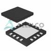
PIC16F1575-E/JQ
Microchip Technology
IC MCU 8BIT 14KB FLASH 16UQFN
OPA4354AIPWR
Texas Instruments
IC CMOS 4 CIRCUIT 14TSSOP
P6SMB33A
Bourns Inc.
TVS DIODE 28.2VWM 45.7VC DO214AA
GCM1885C1H4R4CA16D
Murata Electronics
CAP CER 4.4PF 50V C0G/NP0 0603
R5F100LGAFB#10
Renesas Electronics America Inc
IC MCU 16BIT 128KB FLASH 64LFQFP -
TC621CCOA
Microchip Technology
THERMOSTAT PROG ACTIVE LOW 8SOIC
IRG4BC20UDPBF
International Rectifier
IGBT, 13A I(C), 600V V(BR)CES, N
MICROSMD175F-2
Littelfuse Inc.
PTC RESET FUSE 6V 1.75A 1210
AC0603KRX7R8BB222
YAGEO
CAP CER 2200PF 25V X7R 0603
1812AA150JAT1A\SB
KYOCERA AVX
CAP CER 15PF 1KV NP0 1812
SY10ELT22ZC
Microchip Technology
IC TRANSLTR UNIDIRECTIONAL 8SOIC
SCW03B-12
MEAN WELL USA Inc.
DC DC CONVERTER 12V 3W
A4840
Sensata-Crydom
SSR RELAY SPST-NO 40A 80-530V
TC4426AEOA
Microchip Technology
IC GATE DRVR LOW-SIDE 8SOIC
C1608NP01H470J080AA
TDK Corporation
CAP CER 47PF 50V NP0 0603
GRM1555C2A8R1DA01J
Murata Electronics
CAP CER 8.1PF 100V C0G/NP0 0402
INA330AIDGST
Texas Instruments
IC OPAMP GP 1 CIRCUIT 10VSSOP
12061C273KAT2A
KYOCERA AVX
CAP CER 0.027UF 100V X7R 1206
74LX1G70CTR
STMicroelectronics
IC BUF NON-INVERT 5.5V SOT323-5
CSNE151-204
Honeywell Sensing and Productivity Solutions
SENSOR CURRENT HALL 90A AC/DC
LF353DT
STMicroelectronics
IC OPAMP JFET 2 CIRCUIT 8SOIC
SMK316B7223KLHT
Taiyo Yuden
CAP CER 0.022UF 630V X7R 1206
R9G01612XX
Powerex Inc.
DIODE GP 1.6KV 1200A DO200AB -
FPF2300MPX
Fairchild Semiconductor
DUAL OUTPUT CURRENT LIMIT SWITCH
HZB6.8MWATL-E
Renesas Electronics America Inc
TVS DIODE 3.5VWM 3CMPAK
P0111MA 1AA3
STMicroelectronics
SCR 600V 800MA TO92-3
88E1545-A1-LKJ2C000
Marvell Semiconductor, Inc.
IC TXRX FULL/HALF 4/4 128LQFP
MAX809SN293D1T1G
onsemi
IC SUPERVISOR 1 CHANNEL SOT23-3
ICL3232IBZ-T
Renesas Electronics America Inc
IC TRANSCEIVER FULL 2/2 16SOIC
EP1K50FI484-2
Altera
LOADABLE PLD, 0.4NS PBGA484
FDMF6824C
onsemi
IC HALF BRIDGE DRIVER 50A 40PQFN
HVD144AKRF-E
Renesas Electronics America Inc
PLANAR PIN DIODE
MCD56-12IO1B
IXYS
MOD THYRISTOR/DIO 1200V TO-240AA
CD3275A0DRCR
Texas Instruments
PROTOTYPE
SN74ALS240ANSR
Texas Instruments
IC BUFFER INVERT 5.5V 20SO
9FG104EGLF
Renesas Electronics America Inc
IC FREQ TIMING GENERATOR 28TSSOP
MPC8548EVTAUJB
Freescale Semiconductor
MPU, 32-BIT, 1333MHZ, PBGA783
NCP1070STCT3G
onsemi
IC OFFLINE SWITCH FLYBACK SOT223
MIC4422YM
Microchip Technology
IC GATE DRVR LOW-SIDE 8SOIC
BU2510-E3/51
Vishay General Semiconductor - Diodes Division
BRIDGE RECT 1P 1KV 3.5A BU
GS8642Z36GB-167IV
GSI Technology Inc.
IC SRAM 72MBIT PARALLEL 119FPBGA