CD4060 IC: Features, Functions, and Applications Explained
The CD4060 is a highly versatile integrated circuit designed for tasks involving time delays, frequency division, and binary counting. It features a built-in oscillator and a 14-stage binary counter, making it an efficient and straightforward solution for various timing and control applications. With minimal external components, the CD4060 is perfect for creating reliable circuits in both simple and complex setups.Catalog

Introduction to the CD4060 Integrated Circuit
The CD4060 is a CMOS-based, 14-bit binary counter IC that features a built-in oscillator. Part of the CD4000 family, it operates as a versatile complementary metal-oxide-semiconductor (CMOS) integrated circuit. Its primary function is to create customizable time delays, making it a practical choice for timing-related applications.
In addition to time delays, the CD4060 is also capable of generating a range of frequencies. This is made possible by its internal oscillator, which works seamlessly with a few external passive components. This design simplifies its integration into circuits while providing reliable performance.
The CD4060 can also be a great tool for audio or synthesizer enthusiasts. With just one capacitor and two resistors, it can generate ten unique frequencies, opening up a world of creative possibilities.
CD4060 Pin Configuration Explained
The CD4060 is a 16-pin IC designed as a binary counter with a built-in oscillator. Pins Q4 to Q14 serve as outputs, producing a binary count with each positive clock pulse. For oscillator circuits, connections are made to pins nine and ten using external components like resistors and capacitors to control frequency. This straightforward design makes the CD4060 versatile and easy to use in timing or counting applications.
CD4060 Pin Layout Diagram

Detailed Pin Functions of the CD4060
| Pin Name | Pin # | Type | Description |
| VDD | 16 | Power | Supply Voltage (+3 to +15V) |
| GND | 8 | Power | Ground (0V) |
| Q3-Q9 | 1-7 | Output | Counter outputs |
| Q11-Q13 | 13-15 | Output | Counter outputs |
| CEXT | 9 | Input | Connection for external capacitor |
| REXT | 10 | Input | Connection for external capacitor |
| CLK11 | 11 | Input | Clock input/Oscillator pin |
| RST12 | 12 | Input | Resets the counter |
Creating Adjustable Timer Circuits with CD4060
Here's a hands-on example you can construct using the CD4060 chip:

To set up the circuit, you will need a few components. These include a CD4060 chip (such as the CD4060BE model), a rotary switch for timer selection, and resistors and capacitors to control the timing. You'll also need an NPN transistor, a relay, and additional resistors to regulate current flow. Once these components are connected, the circuit begins its operation based on the configured settings.
Using specific values for the capacitor (C1 = 0.22 µF) and resistor (R1 = 100 kΩ), the circuit operates at a frequency calculated by the formula:
Frequency (f) = 1 / (2.3 * C1 * R1)
Substituting the values, you get:
f = 1 / (2.3 * 0.0000022 F * 100000 Ω) = 1.98 Hz
This frequency means the circuit generates nearly two clock pulses per second, which directly impacts the time delay before the outputs go high.
The CD4060's outputs transition to a high state after specific clock pulses, as follows:
• Q3 Timing
The Q3 pin becomes high after 2³ or 8 clock pulses, which equals about 4 seconds.
• Q4 Timing
The Q4 pin reaches a high state after 2⁴ or 16 clock pulses, giving a delay of 8 seconds.
• Q5 Timing
The Q5 pin goes high after 2⁵ or 32 clock pulses, resulting in a delay of 16 seconds.
• Q6 Timing
At Q6, the pin becomes high after 2⁶ or 64 clock pulses, corresponding to a delay of 32 seconds.
• Q7 Timing
The Q7 pin transitions to high after 2⁷ or 128 clock pulses, which is equivalent to 1 minute and 4 seconds.
• Q8 Timing
The Q8 pin becomes high after 2⁸ or 256 clock pulses, leading to a delay of 2 minutes and 8 seconds.
• Q9 Timing
The Q9 pin transitions to high after 2⁹ or 512 clock pulses, giving a delay of 4 minutes and 16 seconds.
• Q11 Timing
At Q11, the output becomes high after 2¹¹ or 2048 clock pulses, resulting in a delay of 17 minutes and 4 seconds.
• Q12 Timing
The Q12 pin goes high after 2¹² or 4096 clock pulses, giving a delay of 34 minutes and 8 seconds.
• Q13 Timing
The Q13 pin becomes high after 2¹³ or 8192 clock pulses, corresponding to a delay of 1 hour, 8 minutes, and 16 seconds.
These timing configurations make the CD4060 suitable for applications that require precise time delays. By adjusting the values of the resistor and capacitor, you can customize the frequency and timing to suit your needs. Whether you’re building a simple timer or a more complex control system, the CD4060 provides flexibility and reliability in its operation.
Understanding the CD4060 Binary Counter and Oscillator
A binary ripple counter is made up of a series of D flip-flops, where the output of one flip-flop connects to the clock input of the next. This setup allows each flip-flop to toggle based on the signal it receives from the one before it. The first flip-flop in the chain serves as the starting point, where the input signal is fed.

In this illustration of a simple 4-bit ripple counter, you see how the output progresses through the chain. However, the CD4060 takes this concept much further by including 14 flip-flops. With this extended arrangement, it can count up to 16,383 steps, the highest possible value for 14 bits.
What makes the CD4060 stand out is its built-in oscillator. This component generates clock pulses without needing an external clock source, which allows the counter to operate on its own. This feature enables the CD4060 to function as a timer, where different Q-outputs correspond to various time intervals or frequencies.
For example, by adjusting the resistor and capacitor values connected to the oscillator, you can set it to produce a 1 Hz clock pulse, meaning the counter increments once every second. If you use the Q3 output, it will toggle to a high state after 8 seconds. On the other hand, selecting Q13 gives a much longer delay of 2 hours and 16 minutes (8,192 seconds). This flexibility makes the CD4060 a useful tool for creating precise time delays or frequency-dividing circuits.
Key Features of the CD4060 Binary Counter
• The CD4060 is a 14-stage binary counter integrated into a compact 16-pin package, available in PDIP, CDIP, SOIC, and TSSOP variations.
• It operates efficiently with a reset propagation delay of 25 nanoseconds at 5V.
• The IC supports nominal voltages of 5V, 10V, and 15V, offering flexibility based on power requirements.
• It covers a counting range of 0 to 16,383, making it versatile for large operations.
• The CD4060 functions within a voltage range of 3V to 18V, accommodating various power environments.
• It combines a binary counter with an oscillator, achieving a maximum clock frequency of 30 MHz at 15V.
• The pin functions are compatible with the TTL series, simplifying integration into existing circuits.
• It operates at a steady medium speed of 8 MHz when powered with 10V, ensuring consistent performance.
• Fully static operation is supported, with buffered inputs and outputs contributing to reliable operation.
• The 16-pin PDIP version includes Schmitt-triggered inputs, enabling unlimited rise and fall times for enhanced usability.
Missing CD4060 Outputs: Q0, Q1, Q2, Q10
You might notice that the CD4060 does not include outputs Q0, Q1, Q2, or Q10. While there’s no official reason provided for this omission, one possible explanation is that the CD4060 was designed as an upgraded version of the CD4040. To accommodate the oscillator and additional features within the same 16-pin design, some outputs may have been excluded.
How the CD4060 Operates
The CD4060 Integrated Circuit is designed to work seamlessly as both a binary counter and an internal oscillator. It progresses with each clock pulse, increasing the counter value by one whenever there is a negative shift in the clock pulse. This counting is done in binary numbers, making it efficient for various timing and counting applications.
To keep the chip functioning properly, you must connect the reset pin to the ground or the negative supply voltage. This ensures that the counter and oscillator operate smoothly without interruptions.
When you apply a high signal, often referred to as ""1"" or ""HIGH,"" to the reset pin, it instantly resets the oscillator and counter back to zero. This feature is handy when you need to restart the timing or counting process from the beginning.
| Truth Table | Reset | Counter Value |
| X (don't care condition) | 1 | Resets the oscillations to 0 |
| Negative transitions | 0 | |
| Positive transition | 0 | There is no change in the counter value |
The Boolean logic table above illustrates how the reset value and clock pulse interact. It shows how the counter behaves in response to different signals, making it easier to understand and control the chip's operation.
Best Applications for the CD4060 IC
The CD4060 is a versatile chip that combines an oscillator and a counter, making it a great choice for tasks that need accurate and adjustable timing. Its design allows it to handle time delays efficiently, making it a popular option for timing-related projects. Whether you’re building a circuit to create time delays or need to divide a signal into smaller segments, the CD4060 fits the job.
This IC is particularly useful for creating dependable time-delay circuits with very few extra components, making it simple to set up and use. It’s built as a 14-bit binary counter with 12 output pins labeled from Q1 to Q14, except for Q2 and Q3. These pins generate a binary count when clock pulses are sent into the chip. As the binary count increases, it allows for a wide range of timing options, from short to very long durations.
If you’re looking for a solution to work with timing or frequency-based projects, the CD4060 offers a straightforward and reliable way to achieve results. Its ability to count from 0 to 16383 in binary form, triggered by incoming clock pulses, makes it ideal for applications requiring precision without overcomplicating your design.
Working Mechanism of the CD4060
The CD4060 integrated circuit has a built-in oscillator that works seamlessly with its binary counter. This combination allows the IC to count up by one in binary format each time the clock pulse transitions to a lower state, or ""falls."" This behavior makes it a reliable tool for time-based applications.
For the circuit to work properly, the reset pin must always be connected to the ground or the negative power supply. If this pin receives a positive signal (often called HIGH or ""1""), the counter or oscillator stops and returns to its starting point. Essentially, the reset pin acts as a restart button, ensuring the circuit begins again from zero when triggered.
| Truth Table | Reset | Counter Value |
| X | 1 | Resets Counter to 0 |
| Negative transition | 0 | |
| Positive transition | 0 | No change |
Steps to Set the Oscillator Frequency on CD4060
To configure the oscillator frequency in the CD4060, you’ll need to use external components like resistors and capacitors. These components directly affect how the internal oscillator functions. Specifically, the frequency depends on the capacitance of a capacitor connected to pin 11 and the resistance values tied to pins 9 and 10. Adjusting the values of these components lets you modify the time delay or the oscillation frequency to suit your needs.
When setting up the circuit, it's helpful to keep in mind that the resistor at pin 11 should be about ten times larger than the resistor at pin 10. This ensures smooth operation. The unconnected terminals of the capacitor and resistors are joined together to complete the circuit, as shown in the Proteus schematic.
To calculate the frequency, you can use this simple formula:
f = 1 / (2.5 x R1 x C1)

For example, if you choose R1 to be 1M ohm and C1 to be 0.22µF, the calculation will look like this:
f = 1 / (2.5 * 1,000,000 * 0.00000022)
f = 1.8 Hz
This means the oscillator will produce a clock frequency of 1.8Hz with these values. To find the clock period, you simply take the inverse of the frequency:
1/f = 0.56 seconds
It's worth noting that while the oscillator operates at this frequency, the output pins switch states at intervals that are multiples of the oscillator's period. This behavior is further explained when analyzing the timing of the output pins.

Once the circuit is powered, the oscillator will begin working immediately. If you need to stop or reset it, you can apply a logic HIGH or positive signal to the RESET pin. This will halt the oscillation and reset the system to its initial state, ready to start again when needed.
Timing Calculation for CD4060 Output Pins
To figure out the timing of the output pins in the CD4060, you can rely on a simple frequency relationship: each pin operates at half the frequency of the one before it. For example, if pin 3 works at 4Hz, pin 2 will double that at 8Hz. This predictable behavior helps you estimate the time intervals for each output.
The timing can be calculated using the formula:
T = 2n / fosc
Here, T represents the time period for the pin, fosc is the oscillator's frequency, and n is the output pin number. Let’s say you want to calculate the timing for pin Q6, with n being 6 and the oscillator frequency (fosc) set at 1.8Hz:
T = 26 / 1.8
T = 64 / 1.8
T ≈ 35.5 seconds
This calculation means that pin Q6 will switch to a high state after about 35.5 seconds. Each pin follows this formula, making it easy to determine the timing for various outputs by just substituting the respective n value. This clear pattern ensures you can plan delays and outputs effectively for your application.
Practical Guide to Using the CD4060
To set up the CD4060, start by connecting the VDD pin to the positive terminal of your power supply and the GND pin to the negative terminal. The IC can handle supply voltages from 3V to 15V, and some versions even go up to 20V, so always check your datasheet for the specific model you're using.
To activate the oscillator, you'll need to connect a resistor to the REXT pin, a capacitor to the CEXT pin, and another resistor to the CLK pin. These components should meet at a common point as shown in the configuration diagram.
The frequency is determined using the formula:
Frequency (f) = 1 / (2.3 × Ct × Rt)
For accurate results, ensure that Rt is significantly smaller than the second resistor (R2).
If you need to reset the chip, apply a HIGH signal to the RST (Reset) pin. When this pin is LOW, the chip operates normally, but a HIGH signal will bring the count back to zero.
The outputs from the Q pins can be used to control various operations, with each pin reaching a HIGH state after a specific number of clock pulses:
• Q3 reaches HIGH after 2³ pulses, equivalent to 8 clock cycles.
• Q4 achieves HIGH after 2⁴ pulses, corresponding to 16 clock cycles.
• Q5 hits HIGH after 2⁵ pulses, encompassing 32 clock cycles.
• Q6 attains HIGH after 2⁶ pulses, spanning 64 clock cycles.
• Q7 ascends to HIGH after 2⁷ pulses, encompassing 128 clock cycles.
• Q8 elevates to HIGH after 2⁸ pulses, covering 256 clock cycles.
• Q9 rises to HIGH after 2⁹ pulses, spanning 512 clock cycles.
• Q11 attains HIGH after 2¹¹ pulses, encompassing 2048 clock cycles.
• Q12 hits HIGH after 2¹² pulses, spanning 4096 clock cycles.
• Q13 ascends to HIGH after 2¹³ pulses, covering 8192 clock cycles.
Enhancing Precision with Crystals on CD4060
Using a crystal with the CD4060 can improve the precision of its oscillator. This setup is commonly referred to as a Pierce Oscillator and is ideal for applications requiring accurate timing or frequency generation.
Although the CD4060's datasheet doesn't provide extensive guidance on choosing component values for this configuration, similar chips like the 74AHC1G4210 offer some useful insights. For example, the 74AHC1G4210 datasheet suggests using a power-regulating resistor, R1, to stabilize the oscillator's operation against variations in supply voltage or current.
To ensure the oscillator starts and continues oscillating reliably, the transconductance of the circuit must be sufficient. This means that R1 should not have a very high value. As a general guideline, a resistor value around 2.2 kΩ is practical for many crystal oscillator setups, balancing stability and reliable performance.
This approach ensures the crystal-based oscillator operates smoothly, delivering a stable frequency for your CD4060 circuit.

Choosing the Right Crystal for CD4060
Choosing the right crystal for the CD4060 depends on the output frequency you want to achieve. If you aim to use the IC as a frequency divider to produce a steady 500 Hz output, the crystal frequency must align with the division ratios of the CD4060's output pins.
The timing of each pin follows a pattern where Q3 requires 8 clock pulses for a high state and another 8 for a low state, resulting in a total of 16 pulses per cycle. This pattern is consistent across all outputs, allowing you to calculate the required crystal frequency for 500 Hz output at different pins:
• Q3: 500 Hz × 16 pulses = 8 kHz
• Q4: 500 Hz × 32 pulses = 16 kHz
• Q5: 500 Hz × 64 pulses = 32 kHz
• Q6: 500 Hz × 128 pulses = 64 kHz
• Q7: 500 Hz × 256 pulses = 128 kHz
• Q8: 500 Hz × 512 pulses = 256 kHz
• Q9: 500 Hz × 1024 pulses = 512 kHz
• Q11: 500 Hz × 4096 pulses = 2.048 MHz
• Q12: 500 Hz × 8192 pulses = 4.096 MHz
• Q13: 500 Hz × 16384 pulses = 8.192 MHz
While some of these crystal frequencies might not be readily available, commonly used values like 2.048 MHz and 4.096 MHz are ideal choices for achieving a 500 Hz output. This flexibility lets you select a crystal that matches both your desired frequency and what's accessible, ensuring the CD4060 functions effectively in your application.
CD4060-Based Street Light Control System
In this example, the CD4060 is used to create a street light control system with a built-in 6-hour delay. The setup integrates a Light-Dependent Resistor (LDR) connected to the reset pin, which helps monitor the surrounding light levels. When the light falls below a specific threshold, the LDR sends a signal to reset the timer.
Once the reset is triggered, the CD4060 begins counting, and after a delay of 6 hours, the connected LED lights are turned on. This timing delay is achieved by carefully configuring the crystal oscillator frequency to match the desired timing interval.

CD4060 Alternatives and Equivalent ICs
You can explore the following alternatives and equivalents for the CD4060:
• CD4060 (various manufacturers, such as NTE4060, MC14060, HCF4060, TC4060, HEF4060)
• 4020: A 14-stage binary ripple counter (no built-in oscillator)
• 4024: A 7-stage binary ripple counter (no built-in oscillator)
• 4040: A 12-stage binary ripple counter (no built-in oscillator)
• CD4024B: Available in 7-bit and 12-bit configurations, which can serve as viable substitutes
These alternatives may require you to design an external oscillator if one is not included in the IC.
CD4060 IC Applications in Real-World Scenarios
Timing Devices
The CD4060 is ideal for creating systems that require accurate and consistent time tracking. It’s widely used in both industrial and consumer electronics because of its ability to generate precise timing intervals. Whether you’re designing a timer circuit or managing time-sensitive operations, this IC simplifies the process with its built-in oscillator and counter functionality.
Delay-Inducing Circuits
When you need to introduce significant delays in your circuit, the CD4060 is a reliable choice. It is especially useful for applications like home security systems or automated industrial processes where precise delays are critical. Its ability to deliver long time intervals with minimal components makes it a convenient option for various designs.
Frequency Divider
The CD4060 excels at dividing high-frequency signals into smaller, more manageable segments. This feature is particularly useful in audio and communication systems, where adjusting frequency levels is necessary for proper operation. The IC’s built-in counter simplifies the division process, saving time and reducing the need for additional components.
Event Counters
The CD4060 is also effective in applications where counting events or operations is required. From basic counting tasks to complex industrial monitoring systems, it provides reliable performance. Its versatility makes it a go-to solution for projects involving event tracking or sequential operations.
The CD4060's broad range of applications demonstrates its flexibility and usefulness, making it a dependable choice for time-related, frequency management, and event-counting tasks.
About the Manufacturer of CD4060
Texas Instruments (TI) is a global leader in the semiconductor industry, known for its innovative contributions to technology. Operating in 35 countries, the company brings together a vast team of talented individuals. TI's journey began in 1958 when one of its employees created the first working integrated circuit, a groundbreaking achievement that laid the foundation for modern electronics.
Conclusion
The CD4060 is a versatile IC that combines an oscillator and a binary counter to handle a wide range of timing and frequency-related tasks. Whether you need precise time delays, frequency division, or reliable event counting, the CD4060 delivers consistent and easy-to-use functionality. Its flexible design and wide applications make it a valuable tool for creating dependable circuits in various projects
About us
ALLELCO LIMITED
Read more
Quick inquiry
Please send an inquiry, we will respond immediately.
Frequently Asked Questions [FAQ]
1. What is the operating voltage range of the CD4060?
The CD4060 operates within a voltage range of 3V to 18V, making it suitable for various applications. However, it is most commonly used at 5V for standard setups.
2. How much does the CD4060 IC cost?
The price of the CD4060 IC can vary depending on the supplier and region. You can check platforms like Jotrin for the most up-to-date pricing details.
3. How does a Pierce oscillator function?
A Pierce oscillator works by using a crystal to control the oscillation frequency. The crystal operates at its series resonant frequency, ensuring precise oscillation. In this setup, the circuit creates a low-impedance path between the output and input, and the resonance causes a 180-degree phase shift. This phase shift helps maintain positive feedback, allowing the oscillator to function smoothly.
4. How many pulses does the CD4060 binary counter count before activating the circuit?
The CD4060 binary counter counts 16 pulses before the circuit turns on. This mechanism is part of its built-in binary counting functionality.
5. How does the CD4060 work as a timer circuit?
The CD4060 can be configured as a basic timer to create delayed shutdowns. The timer can be adjusted to provide delays ranging from 1 to 2 hours or even longer. When used this way, the circuit powers the load initially and automatically switches it off once the set delay time is completed.
74LS vs. 74HC: Which Logic IC Series is Right for You?
on November 29th
TDA7377 vs TDA7379: Which Amplifier Suits Your Audio Needs?
on November 29th
Popular Posts
-

Complex Instruction Set Computers: How They Changed Computing?
on April 18th 147749
-

USB-C Pinout and Features
on April 18th 111919
-

Using Xilinx Unified Simulation Primitives: A Comprehensive Guide to FPGA Design and Simulation
on April 18th 111349
-

Power Supply Voltages in Electronics: Meaning of VCC, VDD, VEE, VSS, and GND
on April 18th 83714
-

RJ45 Connector Guide: Pinout, Wiring, Cable Types, and Uses
on January 1th 79502
-

The Ultimate Guide to Wire Color Codes in Modern Electrical Systems
The way our electrical systems use colors isn’t just for looks. Each wire color now indicates a specific function, making it easier to identify and handle electrical components correctly during ins...on January 1th 66872
-

Quality (Q) Factor: Equations and Applications
The quality factor, or 'Q', is important when checking how well inductors and resonators work in electronic systems that use radio frequencies (RF). 'Q' measures how well a circuit minimizes energy...on January 1th 63005
-

Purge Valve Guide: Function, Symptoms, Testing, and Replacement for Optimal Engine Performance
The purge valve is a key part of a car’s system that helps keep the air clean by managing fuel vapors before they can escape into the atmosphere. This not only helps the environment by reducing pol...on January 1th 62951
-

Achieving Peak Performance with the Maximum Power Transfer Theorem
The Maximum Power Transfer Theorem explains how energy from a source, such as a battery or generator, flows to a connected load. It shows the exact condition where the load receives the most power....on January 1th 54077
-

A23 Battery Specifications and Compatibility
The A23 battery is a small, cylinder-shaped battery with high voltage. Also called 23A, 23AE, or MN21, it runs at 12 volts and much higher than AA or AAA batteries. Its special design make...on January 1th 52092
HOT Part Number
-

BD9B100MUV-E2
Rohm Semiconductor
IC REG BUCK ADJ 1A 16VQFN
UPD70F3539AF5A9-PN7-Q-A
Renesas Electronics America Inc
IC MICROCONTROLLER
18081A621JAT2A
KYOCERA AVX
CAP CER 620PF 100V NP0 1808
FDN340P
onsemi
MOSFET P-CH 20V 2A SUPERSOT3
70231-101
Amphenol ICC (FCI)
CONN RCPT BLADE PWR 8POS EDGE MT
MPSW42RLRAG
onsemi
TRANS NPN 300V 0.5A TO92
MC7824BT
onsemi
IC REG LINEAR 24V 1A TO220AB
AD8009ARZ-REEL
Analog Devices Inc.
IC OPAMP CFA 1 CIRCUIT 8SOIC
LT1815CS5#TRPBF
Analog Devices Inc.
IC OPAMP VFB 1 CIRCUIT TSOT23-5
DG411DYZ
Renesas Electronics America Inc
IC SWITCH SPST-NCX4 35OHM 16SOIC
VFT2060C-M3/4W
Vishay General Semiconductor - Diodes Division
DIODE SCHOTTKY 20A 60V ITO-220AB
TSX562AIYST
STMicroelectronics
IC CMOS 2 CIRCUIT 8MINISO
MR256D08BMA45
Everspin Technologies Inc.
IC RAM 256KBIT PARALLEL 48FBGA
VSC3312YYP-01
Microchip Technology
IC SWITCH 16X16 6.5GBPS 196FCBGA
XC68HC908GP20CFB
Motorola
TSG 8BIT20K FLASH
CSR8811A08-ICXR-R
Qualcomm
IC RF TXRX+MCU BLUETOOTH
MPSW05
onsemi
TRANS NPN 60V 0.5A TO92
1N4055R
Solid State Inc.
DIODE GEN PURP REV 900V 275A DO9 -

ASX342ATSC00XPED0-DP
onsemi
IMAGE SENSOR VGA 1/4 CIS SOC
0433.125NR
Littelfuse Inc.
FUSE BOARD MNT 125MA 125VAC/VDC
1SMA5941BT3G
onsemi
DIODE ZENER 47V 1.5W SMA
DCP010512BP-U/700
Texas Instruments
DC DC CONVERTER 12V 1W
1-1734344-1
TE Connectivity AMP Connectors
CONN D-SUB HD RCPT 15P R/A SLDR
KSD1621STF
onsemi
TRANS NPN 25V 2A SOT89-3
BQ24161RGET
Texas Instruments
IC BATT CHG LI-ION 1CELL 24VQFN
BTA26-600BW
STMicroelectronics
TRIAC ALTERNISTOR 600V 25A TOP3
NCP1239DD65R2G
onsemi
IC OFFLINE SWITCH FLYBACK 7SOIC
TMS320TCI6482BZTZA
Texas Instruments
TMS320 - DIGITAL SIGNAL PROCESSO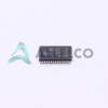
BQ20Z90DBTR-V150
Texas Instruments
IC GAS GAUGE LI-ION 30TSSOP
PCMB104T-1R0MT
Susumu
FIXED IND 1UH 18A 3.3 MOHM SMD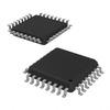
CY29942AXCT
Infineon Technologies
IC CLK BUFFER 1:18 200MHZ 32TQFP
CC0402KRX7R9BB561
YAGEO
CAP CER 560PF 50V X7R 0402
STPS20M60SG-TR
STMicroelectronics
DIODE SCHOTTKY 60V 20A D2PAK
AT25010N-10SC-2.7
Microchip Technology
IC EEPROM 1KBIT SPI 3MHZ 8SOIC
04023A1R0CAT4A
KYOCERA AVX
CAP CER 1PF 25V C0G/NP0 0402
ISL6327IRZ
Intersil
SWITCHING CONTROLLER, VOLTAGE-MO -

LQW18AN75NG0ZD
Murata Electronics
FIXED IND
DFA100BA160
SanRex Corporation
DIODE MODULE 1600V 100A
BAR46AFILM
STMicroelectronics
DIODE ARRAY SCHOTTKY 100V SOT23
MAX825SEUK
Analog Devices Inc./Maxim Integrated
IC SUPERVISOR MPU
MMST2222A-7-F
Diodes Incorporated
TRANS NPN 40V 0.6A SOT323
FODM8801AR2
onsemi
OPTOISO 3.75KV TRANS 4-MINI-FLAT
FJV1845FMTF
Fairchild Semiconductor
SMALL SIGNAL BIPOLAR TRANSISTOR,
EVK105RH5R1JW-F
Taiyo Yuden
CAP CER 5.1PF 16V R2H 0402
6651170-3
TE Connectivity AMP Connectors
CONN EDGE DUAL FMALE 4POS 0.508
KSZ8893FQLI-FX
Microchip Technology
IC SWITCH ETH 3PORT 128QFP
170M6340
Eaton - Bussmann Electrical Division
FUSE SQUARE 400A 1.3KVAC RECT
BCM20741A2KFB1G
Broadcom Limited
SINGLE-CHIP BLUETOOTH
MAX3443EASA+
Analog Devices Inc./Maxim Integrated
IC TRANSCEIVER HALF 1/1 8SOIC
GRM0335C1H9R3DA01D
Murata Electronics
CAP CER 9.3PF 50V C0G/NP0 0201
TNY175PN
Power Integrations
11.5 W (85-265 VAC) 15 W (230 VA
742700726
Würth Elektronik
FERRITE CORE 278 OHM SOLID 4MM
DM74S20N
onsemi
IC GATE NAND 2CH 4-INP 14DIP
P4SMA56CA-E3/61
Vishay General Semiconductor - Diodes Division
TVS DIODE 47.8VWM 77VC DO214AC