
Comprehensive Overview of the 7408 Logic Gate IC
The 7408 IC is a versatile logic gate chip designed for various digital applications. It houses four independent 2-input AND gates, making it a reliable choice for building circuits that require logical operations. Whether you’re creating simple systems or more complex designs, this IC offers flexibility and ease of use, ensuring efficient performance and straightforward integration.Catalog

Overview of 7408 Integrated Circuit
The 7408 IC is a compact chip that contains four two-input AND gates. It is designed to make it easier to create and work with digital systems. Each gate has two inputs and one output, performing a basic logic operation that helps in building circuits for various applications.
This IC is widely used because it simplifies the process of designing digital circuits. Whether you're working on a small project or a more complex system, the 7408 provides a reliable way to implement logic operations. Its versatility allows it to be paired with other components, giving you the ability to create a wide range of electronic solutions. The design of the chip also ensures that it can be integrated smoothly into projects, whether you're an engineer or a hobbyist exploring the world of electronics.
Key Features of 7408 Integrated Circuit
Compatibility with Various Logic Families
The 7408 IC is designed to work seamlessly with TTL logic, making it a versatile choice for different types of circuits. Its ability to directly interface with CMOS, NMOS, and other TTL outputs ensures that it can be integrated into a wide range of systems without any hassle.
Four Independent AND Gates
This IC includes four separate two-input AND gates. Each gate operates independently, giving you the flexibility to use them for multiple tasks within the same circuit. This setup is particularly useful when designing systems that require multiple logic operations.
Operates Across a Wide Voltage Range
The IC operates effectively within a broad voltage range, allowing it to be used in various power configurations. Whether your system runs on lower or higher voltage levels, the 7408 is built to handle it reliably.
Low Power Consumption
One of the advantages of the 7408 IC is its efficient design, which ensures low power usage. This feature makes it an excellent choice for systems where conserving energy is a priority, especially in battery-operated devices.
High Noise Immunity
The IC is built to resist interference from electrical noise, ensuring stable and consistent operation. This means your circuit will function as intended, even in environments where noise could be a concern.
Fast Switching Speed
The 7408 IC is designed for quick performance, with rapid switching speeds that allow for efficient signal processing. This feature is especially useful in applications requiring quick responses and high-speed operations.
Overload Protection
The IC includes features to prevent damage from excessive current or voltage, which helps prolong its lifespan. This protective capability ensures that your circuit remains safe during unexpected changes in power conditions.
Minimal Noise Levels
In addition to its high noise immunity, the IC generates minimal internal noise during operation. This results in cleaner signal processing and better performance for your circuits.
Multiple Input and Output Lines
With eight input lines and four output lines, the IC provides ample connectivity options. This setup gives you the flexibility to design circuits that require multiple connections without any complexity.
Technical Specifications of 7408 Integrated Circuit
| Parameter | Value |
| Logic Family | TTL |
| Number of Gates | Quad 2-Input AND |
| Dual-In-Line (DIL) | 14 pin |
| Independent 2-Input AND Gates | 4 |
| Supply Voltage (VCC) | 4.75V to 5.25V |
| High-Level Input Voltage (VIH) | 2V (min) |
| Low-Level Input Voltage (VIL) | 0.8V (max) |
| High-Level Output Voltage (VOH) | 2.7V (min) |
| Low-Level Output Voltage (VOL) | 0.5V (max) |
| Input Current (IIH/IIL) | ±20µA (max) |
| Output Current (IOH/IOL) | ±8mA (max) |
| Propagation Delay (tpd) | 11ns (typical) |
| Operating Temperature Range | 0°C to 70°C |
| Package | Dual In-line Package (DIP) |
Pinout Diagram of 7408 IC
The 7408 IC has fourteen pins, each serving a specific function. These include pins for ground (GND) and power supply (Vcc). Pin 1 acts as the first input for the first AND gate, pin 2 serves as the second input, and pin 3 delivers the output for this gate. Similarly, pins 4 through 6 handle the inputs and output for the second AND gate.
Pin 7 is designated as the ground connection, ensuring the chip is powered properly. On the opposite end, pin 14 serves as the Vcc pin, which provides the required power for the chip to operate effectively.

The diagram of the 7408 IC uses "A" and "B" to indicate the inputs for each gate, while "Y" represents the output. "GND" and "VCC" highlight the ground and power supply connections, helping you understand how the chip integrates into a circuit.
Pin Configuration of 7408 IC
| Pin No. | Pin Name | Description |
| 1 | A Input Gate 1 | Input of the first AND gate (Input A1) |
| 2 | B Input Gate 1 | Input of the first AND gate (Input B1) |
| 3 | Y Output Gate 1 | Output of the first AND gate |
| 4 | A Input Gate 2 | Input of the second AND gate (Input A2) |
| 5 | B Input Gate 2 | Input of the second AND gate (Input B2) |
| 6 | Y Output Gate 2 | Output of the second AND gate |
| 7 | Ground | Ground (Common Ground for all gates) |
| 8 | Y Output Gate 3 | Input of the third AND gate (Input A3) |
| 9 | B Input Gate 3 | Input of the third AND gate (Input B3) |
| 10 | A Input Gate 3 | Output of the third AND gate |
| 11 | Y Output Gate 4 | Positive Power Supply |
| 12 | B Input Gate 4 | Input of the fourth AND gate (Input A4) |
| 13 | A Input Gate 4 | Input of the fourth AND gate (Input B4) |
| 14 | Vcc - Positive Supply | Output of the fourth AND gate |
Truth Table for IC 7408
The 7408 IC contains four 2-input AND gates and operates according to a simple truth table that reflects the basic logic of an AND gate.
| A (Input) | B (Input) | Y (Output) |
| 0 | 0 | 0 |
| 0 | 1 | 0 |
| 1 | 0 | 0 |
| 1 | 1 | 1 |
In the table:
• "A" and "B" are the two inputs for each AND gate.
• "Y" represents the output of the gate.
• "0" and "1" indicate low (0V) and high (typically 5V in TTL logic) voltage levels, respectively.
The output (Y) of an AND gate becomes high (1) only when both inputs (A and B) are high (1). If either or both inputs are low (0), the output remains low (0). This behavior is consistent across all four AND gates in the 7408 IC.
Equivalent Options for IC 7408
• SN7408: Equivalent to the 7408, part of the Texas Instruments SN series
• 74LS08: Low-power Schottky version with faster switching and lower power consumption
• 74HC08: High-speed CMOS version with broader voltage range and faster operation
• 74HCT08: High-speed CMOS with inputs compatible with TTL logic
• CD4081: CMOS version supporting a voltage range of 3V to 18V
• MC14008: CMOS version similar to CD4081, designed for higher voltage applications
Manufacturers of 7408 Integrated Circuit
The 7408 IC is part of the widely used 74xx series of digital logic integrated circuits. This series includes a variety of ICs, each designed to perform specific logic functions. The 7408, in particular, is a quad 2-input AND gate containing four AND gates, each with two inputs.
Several semiconductor companies manufacture the 7408 IC and other ICs in the 74xx series:
• Texas Instruments (TI): A leading semiconductor company known for producing a wide range of ICs, including those in the 74xx series.
• Fairchild Semiconductor: Now part of ON Semiconductor, Fairchild was one of the first companies to produce 74xx series ICs.
• NXP Semiconductors: Formerly Philips Semiconductors, NXP is a well-known manufacturer of 74xx series logic ICs.
• STMicroelectronics: A global semiconductor manufacturer producing various ICs, including those from the 74xx series.
Though the 7408 IC may vary slightly between manufacturers, versions are typically interchangeable as long as they meet the standard specifications of the 74xx series.
Applications of 7408 IC
Digital Logic Gates
The 7408 IC is widely used to implement digital logic gates in circuits. Its AND gates are ideal for performing basic logic operations in digital systems.
Binary Counters
This IC plays a role in binary counters by helping process signals that increment or decrement a binary count. It ensures accurate counting in digital applications.
Multiplexers
Multiplexers rely on logic gates like those in the 7408 to combine multiple input signals into a single output. The IC ensures smooth signal selection and processing.
Flip-Flops
The 7408 is often used in the design of flip-flops, which are essential for creating memory elements in digital systems. It helps store and toggle binary data efficiently.
Bus Driver/Receiver
In data buses, this IC acts as a driver or receiver, enabling reliable data transfer between components without interference or signal loss.
Address Decoders
The IC is also used in address decoding, a process that ensures proper routing of signals to specific memory or hardware locations in digital devices.
Data Latches
7408 ICs can help create data latches, which temporarily store data for processing. This makes them valuable in timing-sensitive applications.
Logic Gate Circuits
This IC forms the backbone of many logic gate circuits, providing consistent and reliable logic operations for complex designs.
Decoders
Decoders use AND gates like those in the 7408 IC to convert binary inputs into specific outputs, ensuring accurate signal decoding.
Shift Registers
Shift registers require precise logic operations, and the 7408 IC aids in shifting and storing data effectively within these systems.
Counters
This IC contributes to various counter designs by providing the logic required for counting processes in digital devices.
Arithmetic Circuits
The IC is used in arithmetic circuits to perform basic operations like addition and subtraction, supporting the design of computational systems.
Memory Units
In memory units, the IC assists in managing data flow and storage, ensuring seamless read and write operations.
Measuring Instruments
7408 ICs are used in measuring instruments to process signals and provide accurate readings, ensuring reliable measurements.
Servers
Servers utilize the IC for managing data flow and performing logic operations, enhancing their efficiency and processing capabilities.
ALUs (Arithmetic Logic Units)
The IC is an integral part of ALUs, helping perform both arithmetic and logic operations in processors and digital systems.
Control Systems
In control systems, the IC ensures logical decision-making and smooth execution of automated processes.
Input/Output Interface
This IC helps manage input and output interfaces by controlling data transfer between devices and ensuring proper signal routing.
Signal Gating
Absolute Maximum Ratings for 7408 IC
The 7408 IC is ideal for signal gating, where it controls and directs the flow of signals within a circuit, enhancing overall system performance.
| Supply Voltage | 7V |
| Input Voltage | 5.5V |
| Operating Free Air Temperature | 0°C to +70°C |
| Storage Temperature Range | -65°C to +150°C |
It is important to adhere to these maximum ratings to ensure the proper functionality and longevity of the 7408 IC. Exceeding these limits can cause damage or lead to degraded performance. By staying within these specified ranges, you can maintain the reliability and performance of the IC in your circuit.
Maximum Propagation Delay
The 7408 IC has a maximum propagation delay of 10 nanoseconds (ns). This is the time it takes for a change in the input to produce a corresponding change in the output. This characteristic is particularly useful for high-speed digital circuits, where timing and synchronization are critical for smooth operation.
Operating Temperature Range
The IC can operate effectively within a wide temperature range of -55°C to 125°C. This allows the chip to perform reliably in a variety of environmental conditions, from extremely cold to very hot temperatures. Such versatility makes it suitable for use in industrial applications as well as in settings that may experience extreme weather conditions or temperature fluctuations.
Storage Temperature Range
The IC can be stored safely within a temperature range of -65°C to 150°C. This ensures that the chip retains its functionality even after being stored for extended periods. Whether in inactive periods or while being transported, this broad storage range protects the IC from potential damage due to unfavorable storage conditions.
High-Speed Operation
The 7408 IC is designed to operate at high speeds, reaching up to 10 MHz. This capability makes it suitable for applications requiring rapid signal processing and quick response times, particularly in high-speed digital systems. Its reliable performance in such scenarios makes it a preferred choice for many engineers and designers.
Recommended Operating Conditions of 7408 IC
| Symbol | Parameter | Min | Typ | Max | Units |
| Vcc | Supply Voltage | 4.75 | 5 | 5.25 | V |
| Vih | HIGH Level Input Voltage | 2 | - | - | V |
| Vil | LOW Level Input Voltage | - | - | 0.8 | V |
| Ioh | HIGH Level Output Current | -0.4 | - | - | mA |
| Iol | LOW Level Output Current | - | - | 16 | mA |
| Ta | Free Air Operating Temperature | 0 | - | 70 | °C |
Electrical Characteristics of 7408 IC
| Symbol | Parameter | Conditions | Min | Typ | Max | Units |
| Vi | Input Clamp Voltage | Vcc = Min, Ii = -12mA | - | - | -1.5 | V |
| Voh | HIGH Level Output Voltage | Vcc = Min, Ioh = MAX, Vih = MAX | 2.4 | 3.4 | - | V |
| Vol | LOW Level Output Voltage | Vcc = Min, Iol = MAX, Vih = MAX | - | 0.2 | 0.4 | V |
| Ii | Input Current @ MAX Input Voltage | Vcc = Max, Vi = 5.5V | - | - | 1 | mA |
| Iih | HIGH Level Input Current | Vcc = Max, Vi = 2.4V | - | - | 40 | µA |
| Iil | LOW Level Input Current | Vcc = Max, Vi = 0.4V | - | - | -1.6 | mA |
| Ios | Short Circuit Output Current | Vcc = Max | -18 | - | -55 | mA |
| Icch | Supply Current with Outputs HIGH | Vcc = Max | - | 4 | 8 | mA |
| Iccl | Supply Current with Outputs LOW | Vcc = Max | - | 12 | 22 | mA |
Switching Characteristics of 7408 IC
| Symbol | Parameter | Conditions | Min | Typ | Max | Units |
| tplh | Propagation Delay Time LOW-to-HIGH | Cl = 15pF, Rl = 400Ω | - | 22 | - | ns |
| tphl | Propagation Delay Time HIGH-to-LOW | Cl = 15pF, Rl = 400Ω | - | 15 | - | ns |
Dimensional Drawing

About us
ALLELCO LIMITED
Read more
Quick inquiry
Please send an inquiry, we will respond immediately.
Frequently Asked Questions [FAQ]
1. What does the "74" in 7408 IC mean?
The "74" in the 7408 IC refers to the series of integrated circuits to which it belongs. Specifically, it is part of the 74xx series, which includes a variety of logic gate ICs. The 7408 is one of these, designed with a quad 2-input AND gate configuration.
2. How is the internal structure of the 7408 IC designed?
The internal structure of the 7408 IC consists of four independent AND gates. Each AND gate has two inputs, labeled as A and B, and one output, labeled as Y. The output (Y) is determined by the logical AND operation applied to the corresponding A and B inputs.
3. What is the main function of the 7408 IC?
The primary function of the 7408 IC is to provide four independent 2-input AND gates within a single chip. It is commonly used to implement logic operations in digital circuits.
4. How does the 7408 IC work?
The 7408 IC works by performing logical AND operations through its four independent gates. Each gate accepts two inputs and produces an output based on the logic of the AND operation, where the output is high only if both inputs are high.
5. How many AND gates are present in the 7408 IC?
The 7408 IC contains four independent 2-input AND gates.
6. Why is the AND gate useful in circuits?
The AND gate is easy to use and serves as a basic building block in digital electronics. It is useful for creating circuits where the output depends on all inputs being active at the same time.
Learn How the 78L05 Voltage Regulator Keeps Your Projects Stable
on November 29th

How IC 7493 Works as a Frequency Divider
on November 29th
Popular Posts
-

Complex Instruction Set Computers: How They Changed Computing?
on June 14th 148402
-

USB-C Pinout and Features
on June 14th 131612
-

Using Xilinx Unified Simulation Primitives: A Comprehensive Guide to FPGA Design and Simulation
on June 14th 111884
-

Power Supply Voltages in Electronics: Meaning of VCC, VDD, VEE, VSS, and GND
on June 14th 94454
-

RJ45 Connector Guide: Pinout, Wiring, Cable Types, and Uses
on January 1th 93984
-

The Ultimate Guide to Wire Color Codes in Modern Electrical Systems
The way our electrical systems use colors isn’t just for looks. Each wire color now indicates a specific function, making it easier to identify and handle electrical components correctly during ins...on January 1th 76891
-

Quality (Q) Factor: Equations and Applications
The quality factor, or 'Q', is important when checking how well inductors and resonators work in electronic systems that use radio frequencies (RF). 'Q' measures how well a circuit minimizes energy...on January 1th 74843
-

Purge Valve Guide: Function, Symptoms, Testing, and Replacement for Optimal Engine Performance
The purge valve is a key part of a car’s system that helps keep the air clean by managing fuel vapors before they can escape into the atmosphere. This not only helps the environment by reducing pol...on January 1th 68783
-

Understanding Capacitors and Their Symbols in Circuit Diagrams
Capacitors are small parts used in almost all electronic devices. They store and release electrical energy and are found in things like power supplies, radios, and circuits that help reduce noise. ...on June 14th 58527
-

A23 Battery Specifications and Compatibility
The A23 battery is a small, cylinder-shaped battery with high voltage. Also called 23A, 23AE, or MN21, it runs at 12 volts and much higher than AA or AAA batteries. Its special design make...on January 1th 58132
HOT Part Number
-
C2012C0G2A222K085AA
TDK Corporation
CAP CER 2200PF 100V C0G 0805
GS1559-CBE2
Semtech Corporation
IC VIDEO RECLOCKER 100BGA
SI5330A-B00202-GM
Skyworks Solutions Inc.
IC CLK BUFFER 1:4 710MHZ 24QFN
VI-200-EX
Vicor Corporation
DC DC CONVERTER 5V 75W
FAN2514S33X
onsemi
IC REG LINEAR 3.3V 200MA SOT23-5
C1608X7R2A102M080AA
TDK Corporation
CAP CER 1000PF 100V X7R 0603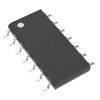
LM339M
Texas Instruments
IC COMPARATOR 4 GEN PUR 14SOIC
UCC5672PWPTRG4
Texas Instruments
IC SCSI 9-LINE TERM 28-HTSSOP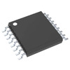
SN74S1051PWR
Texas Instruments
IC 12-BIT BUS TER ARRAY16-TSSOP
62684-501100ALF
Amphenol ICC (FCI)
CONN FPC BOTTOM 50POS 0.5MM R/A
UMK105CG8R2BW-F
Taiyo Yuden
CAP CER 8.2PF 50V C0G/NP0 0402
0603N1R0B101CT
Walsin Technology Corporation
CAP CER 1PF 100V C0G/NP0 0603
LT4321HUF#PBF
Analog Devices Inc.
IC OR CTRLR BRIDGE RECT 16QFN
FQA35N40
Fairchild Semiconductor
MOSFET N-CH 400V 35A TO3P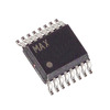
MAX4066ACEE+
Analog Devices Inc./Maxim Integrated
IC SWITCH SPST-NOX4 45OHM 16QSOP
BQ24270RGER
Texas Instruments
IC BATT CHG LI-ION 1CELL 24VQFN
ISL84684IR-T
Renesas Electronics America Inc
IC SWITCH SPDTX2 500MOHM 10TDFN
BCX56-16
Yangjie Technology
Transistors - Bipolar (BJT) - Si -

IRLMS5703TR
Infineon Technologies
MOSFET P-CH 30V 2.3A 6-TSOP
ISL29033IROZ-T7S2722
Renesas Electronics America Inc
OPTICAL SENSOR
1812CC682MAT1A
KYOCERA AVX
CAP CER 6800PF 630V X7R 1812
STUSB4500QTR
STMicroelectronics
IC USB CONTROLLER I2C 24QFN
MIC5319-2.5YD5
Microchip Technology
IC REG LIN 2.5V 500MA TSOT23-5
XCV50E-8CS144C
AMD
IC FPGA 94 I/O 144CSBGA
74CBTLV3253QG
IDT, Integrated Device Technology Inc
IC MUX/DEMULT 2 X 4:1 16QSOP
MBR3045CT
Vishay General Semiconductor - Diodes Division
DIODE ARRAY SCHOTTKY 45V TO220AB
PS9306L-E3-AX
Renesas Electronics America Inc
OPTOISO 5KV 1CH GATE DRVR 6SDIP
QRW025A0A1
ABB Power Electronics Inc.
DC DC CONVERTER 5V 125W
STG3699BVTR
STMicroelectronics
IC SWITCH SPDT X 4 500MOHM 16QFN
FH19SC-17S-0.5SH(05)
Hirose Electric Co Ltd
CONN FFC BOTTOM 17POS 0.5MM R/A
AOZ13987DI-02
Alpha & Omega Semiconductor Inc.
23V USB IDEAL DIODE SWITCH
LTC2626CDD#TRPBF
Analog Devices Inc.
IC DAC 12BIT V-OUT 10DFN
2SC3356-T1B-A
CEL (California Eastern Laboratories)
RF TRANSISTOR NPN SOT-23
SKY87000-11-001
Skyworks Solutions Inc.
IC REG PMIC PWR AMP RF DC 9CSP
CY7C1315KV18-250BZC
Infineon Technologies
IC SRAM 18MBIT PARALLEL 165FBGA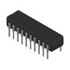
DM74AS240N
Fairchild Semiconductor
IC BUFFER INVERT 5.5V 20DIP -

XR3080XIDTR-F
MaxLinear, Inc.
IC TRANSCEIVER FULL 1/1 14SOIC
DAC7800KUG4
Texas Instruments
IC DAC 12BIT A-OUT 16SOIC
24LC00/SN
Microchip Technology
IC EEPROM 128B I2C 400KHZ 8SOIC
V110C24C100BL
Vicor Corporation
DC DC CONVERTER 24V 100W
06035C471KAT4J
KYOCERA AVX
CAP CER 470PF 50V X7R 0603
DF11-8DP-2DS(52)
Hirose Electric Co Ltd
CONN HEADER R/A 8POS 2MM
HCPL-0730-000E
Broadcom Limited
OPTOISO 3.75KV 2CH DARLNG 8-SO
93LC86T-I/SN
Microchip Technology
IC EEPROM 16KBIT MICROWIRE 8SOIC
R3118N091C-TR-FE
Nisshinbo Micro Devices Inc.
IC SUPERVISOR 1 CHANNEL SOT23-5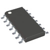
PIC16F1825-E/SL
Microchip Technology
IC MCU 8BIT 14KB FLASH 14SOIC
TPS2410RMST
Texas Instruments
O-RING CONTROLLER
MMSZ5237B_R1_00001
Panjit International Inc.
SOD-123, ZENER
PT7C43390LE
Diodes Incorporated
IC RTC CLK/CALENDAR I2C 8MSOP
LTM8047IY#PBF
Analog Devices Inc.
DC DC CONVERTER 2.5-12V
18121C682KAT2A
KYOCERA AVX
CAP CER 6800PF 100V X7R 1812
74HCT86D,653
NXP USA Inc.
IC GATE XOR 4CH 2-INP 14-SO
GRM1555C1H9R5CA01D
Murata Electronics
CAP CER 9.5PF 50V C0G/NP0 0402
LT1193CS8#TRPBF
Analog Devices Inc.
IC AMP DIFFERENTIAL 8SOIC