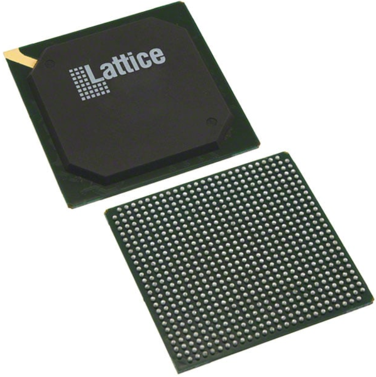
Guide to the FPGA LFE3-35EA-6FN672C from Lattice
The LFE3-35EA-6FN672C from Lattice Semiconductor is an FPGA designed to deliver strong performance while keeping power use low. It provides flexible logic resources, high-speed interfaces, and built-in memory for handling complex digital tasks. With its compact BGA package, it fits easily into space-constrained boards, making it ideal for embedded and communication systems. You can use it to manage control logic, data routing, or signal processing without adding extra hardware. It’s built for reliable operation across a wide temperature range and maintains efficiency even under continuous workloads. Whether used in automation, networking, or IoT, this device helps you create designs that are both powerful and energy-conscious.Catalog
LFE3-35EA-6FN672C Overview
The LFE3-35EA-6FN672C is an FPGA from Lattice Semiconductor’s ECP3 series, designed to balance performance with low power use. It handles a wide range of digital processing tasks while keeping energy consumption low, making it practical for embedded, communication, and industrial applications. You can use it in systems that need efficient logic control, memory resources, and flexible I/O options without drawing much power. Its compact BGA package also helps simplify board design where space is limited.
Looking for LFE3-35EA-6FN672C? Contact us to check current stock, lead time, and pricing.
LFE3-35EA-6FN672C Banks
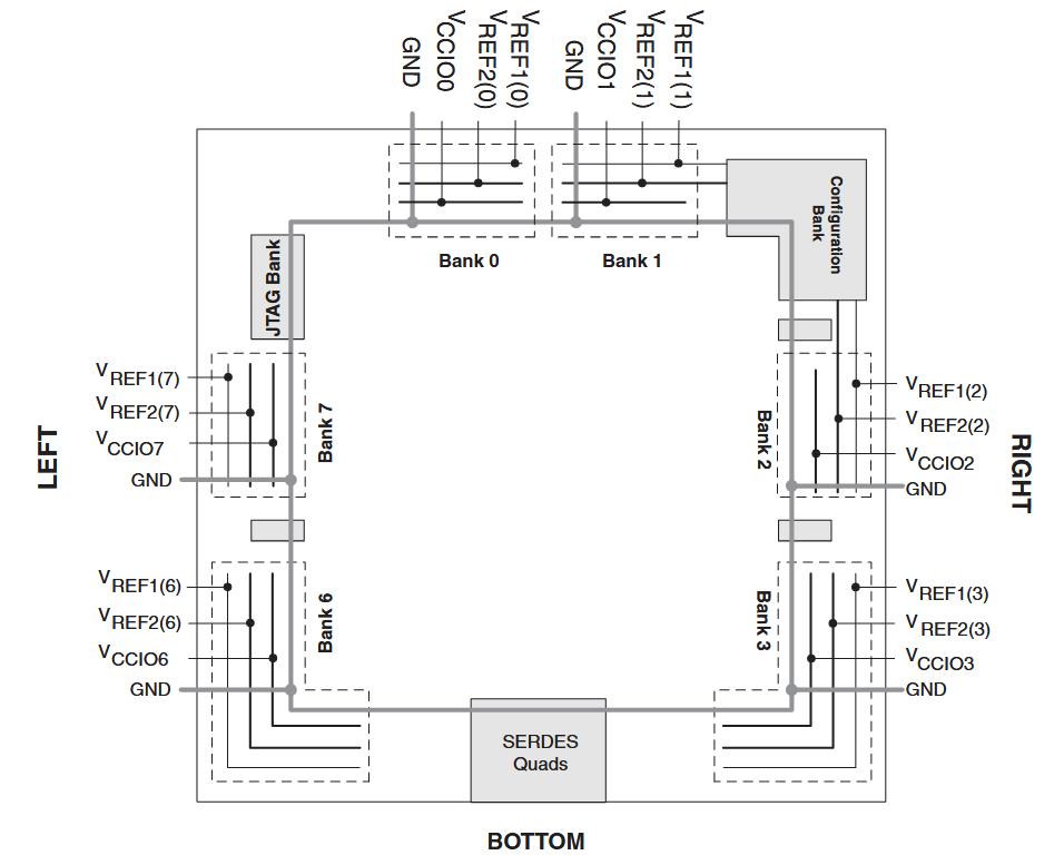
This diagram shows how the I/O banks are arranged around the LFE3-35EA-6FN672C FPGA. Each labeled section, such as Bank 0 through Bank 7, represents a group of input and output pins that connect the chip to other components on a circuit board. The diagram also highlights reference voltage pins (VREF), power pins (VCCIO), and ground connections (GND) placed along the chip edges. At the bottom, the SERDES Quads section handles high-speed serial communication.
Features of LFE3-35EA-6FN672C
High Logic Density for Flexible Design
The LFE3-35EA-6FN672C gives you access to 4,125 Configurable Logic Blocks and 33,000 logic elements, allowing you to build custom digital designs with ease. This flexibility helps you handle complex tasks without needing multiple chips, keeping your setup efficient and compact.
Generous On-Chip Memory
With over 1.3 million RAM bits available, this FPGA lets you store and manage data smoothly within the device. Whether you’re working on signal processing or embedded control, the built-in memory helps maintain fast and reliable performance.
Wide Range of I/O Options
You get 310 user I/O pins, which means you can connect the LFE3-35EA-6FN672C to a variety of external devices and systems. This makes it easier to integrate into existing designs and expand functionality without complicated wiring.
Efficient Low-Voltage Operation
The FPGA operates between 1.14V and 1.26V, helping reduce overall power consumption while maintaining stable performance. You can count on it to run efficiently, especially in applications that demand energy savings or compact power systems.
Reliable Thermal Performance
Designed to function within a temperature range of 0°C to 85°C (TJ), the LFE3-35EA-6FN672C stays dependable even in demanding environments. You can trust it to deliver consistent operation across different conditions.
Compact and Durable Package Design
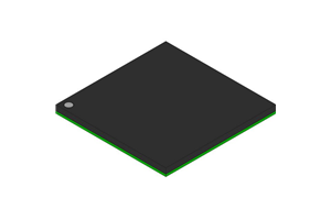
Housed in a 672-FPBGA (27x27) package, this FPGA fits well in space-limited boards. Its fine-pitch layout allows high-density mounting, making it suitable for modern compact electronics.
Easy Surface-Mount Integration
The surface-mount design helps you install the chip securely on your PCB. It provides better mechanical stability and reliable electrical connections, making your final product more durable and consistent.
Optimized for Cost-Effective Performance
As part of Lattice’s ECP3 series, the LFE3-35EA-6FN672C offers a balanced mix of speed, performance, and affordability. It’s built to meet your logic needs without adding unnecessary complexity or cost to your design.
LFE3-35EA-6FN672C Technical Specifications
| Product Attribute | Attribute Value |
| Manufacturer | Lattice Semiconductor |
| Voltage - Supply | 1.14V ~ 1.26V |
| Total RAM Bits | 1358848 |
| Supplier Device Package | 672-FPBGA (27x27) |
| Series | ECP3 |
| Package / Case | 672-BBGA |
| Package | Tray |
| Operating Temperature | 0°C ~ 85°C (TJ) |
| Number of Logic Elements/Cells | 33000 |
| Number of LABs/CLBs | 4125 |
| Number of I/O | 310 |
| Mounting Type | Surface Mount |
| Base Product Number | LFE3-35 |
Simplified Block Diagram of LFE3-35EA-6FN672C
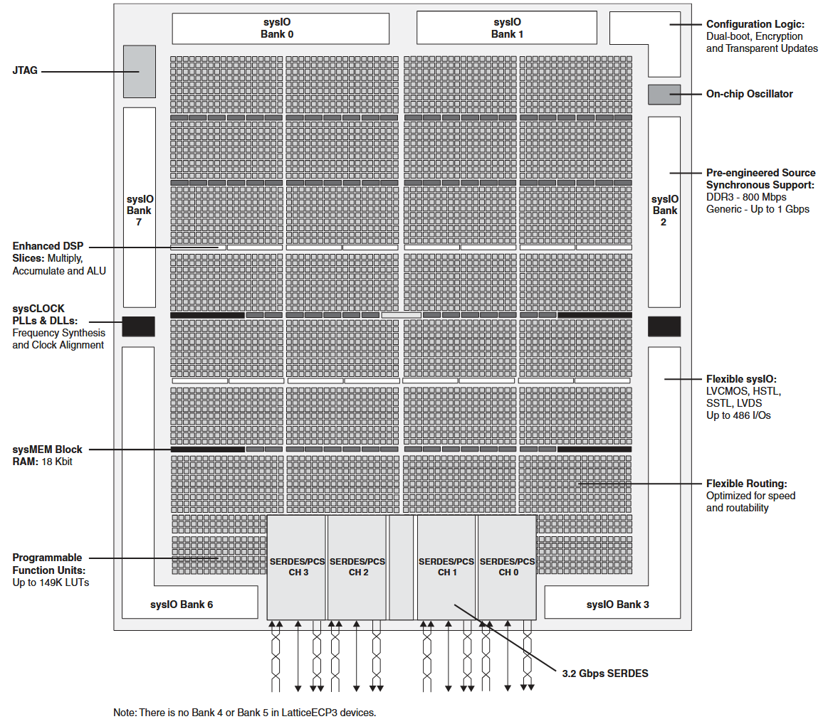
This diagram shows different functional sections like system I/O banks, DSP blocks, memory blocks, and clock management areas arranged in a grid layout. The routing paths connect these sections to allow fast communication across the FPGA. Each labeled area represents parts that handle logic, data storage, and high-speed signal processing. The bottom of the diagram highlights the SERDES channels that support data rates up to 3.2 Gbps, while the sides display input and output interfaces.
PFU Diagram of LFE3-35EA-6FN672C
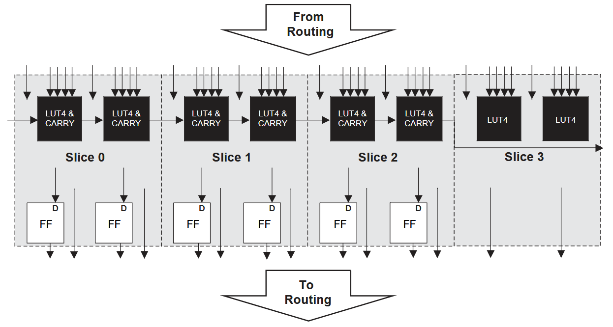
It highlights four slices, labeled Slice 0 through Slice 3, each containing logic elements that process and store data. The first three slices include lookup tables (LUT4s) and flip-flops connected by carry logic, allowing for flexible data handling and arithmetic operations. Slice 3 includes two LUT4s without registers. Arrows labeled “From Routing” and “To Routing” illustrate how signals flow into and out of the PFU, helping different parts of the FPGA communicate efficiently.
Applications of LFE3-35EA-6FN672C
Industrial Automation and Control Systems
The LFE3-35EA-6FN672C works well in industrial automation setups, where you need dependable control logic and smooth communication between devices. You can use it for programmable controllers, motor drivers, and sensor management, helping machines operate efficiently and respond accurately to changing conditions.
Medical Devices and Signal Processing
In medical equipment, this FPGA supports precise data collection and real-time signal processing. It can handle imaging systems, diagnostic tools, and patient monitoring devices, allowing fast response and consistent performance while keeping power use low.
Telecommunications and Networking Equipment
You can use the LFE3-35EA-6FN672C in networking hardware for packet processing, routing, and data control. Its flexible logic structure makes it ideal for base stations, routers, and line cards that need reliable, high-speed communication handling.
Automotive Electronics and Smart Systems
In vehicles, this FPGA supports infotainment systems, driver-assistance features, and in-car communication networks. It helps coordinate multiple electronic functions smoothly, contributing to a better driving experience and more efficient vehicle systems.
Consumer Electronics and Embedded Devices
The LFE3-35EA-6FN672C fits easily into everyday electronic products like smart displays, entertainment systems, and connected home devices. Its low power needs and compact package make it a good match for modern, space-saving designs.
IoT Systems and Edge Control Modules
This FPGA is also a strong choice for IoT applications. It can act as the logic core for gateways, power management systems, or small-scale computing modules. Its efficient design allows you to process data locally, saving energy and improving response time in connected environments.
LFE3-35EA-6FN672C Advantages and Disadvantages
Advantages
• Runs efficiently with a good balance between power use and performance
• Offers flexible logic that fits a wide range of embedded designs
• Works smoothly with Lattice Diamond and Radiant design tools
• Built for reliability and meets ROHS3 environmental standards
• Easy to move between other devices in the same ECP3 family
• Handles signal processing well with low-latency connections and DSP support
• Compact size makes it ideal for tight PCB layouts
Disadvantages
• Has fewer logic elements compared to larger FPGA families like Kintex or Cyclone
• Operates only within a 0°C to 85°C temperature range, limiting outdoor use
• Contains fewer high-speed transceivers for bandwidth-heavy projects
• Requires learning Lattice’s own software tools if you’re used to other platforms
LFE3-35EA-6FN672C Alternatives
| Part Number | Manufacturer | Key Features | Use Case/Notes |
| LFE3-35EA-6FN672I | Lattice Semiconductor | This is an ECP3 FPGA with ~33,000 logic elements, up to 310 I/Os, and supply voltage 1.14 V to 1.26 V. | Good for high-density logic designs where many I/O lines are needed. |
| LFE3-35EA-6LFN672I | Lattice Semiconductor | Similar to above, ~33,000 logic elements, 310 I/Os, same voltage range. The “L” prefix often indicates a low-power variant. | Use in designs where power saving is more critical (e.g. battery-sensitive systems). |
| LFE3-35EA-6FTN256C | Lattice Semiconductor | ECP3 FPGA with ~33,000 logic elements, 133 I/Os, supply 1.14 V to 1.26 V, in a 256-pin ftBGA package. | Useful when fewer I/O pins are needed and a smaller package is preferred (e.g. space constrained boards). |
About Lattice Semiconductor
Lattice Semiconductor is a trusted name in programmable logic devices, known for creating solutions that balance performance and power efficiency. The company focuses on making flexible, easy-to-use products that fit a wide range of applications, from communication systems to consumer electronics. When you choose a Lattice device like the LFE3-35EA-6FN672C, you get technology built with reliability and long-term use in mind. Lattice continues to design compact and efficient FPGAs that help you bring new ideas to life while keeping designs simple and practical.
Conclusion
The LFE3-35EA-6FN672C gives you a practical mix of speed, flexibility, and efficiency in one chip. Its high logic density and on-chip memory let you handle many digital operations within a compact form. With strong I/O support and low power needs, it fits well in automation, communication, and IoT projects. You can depend on it for steady performance even in demanding systems. This FPGA helps you simplify your setup without giving up control or reliability. It’s a smart option when you need dependable performance in energy-efficient designs.
About us
ALLELCO LIMITED
Read more
Quick inquiry
Please send an inquiry, we will respond immediately.
Frequently Asked Questions [FAQ]
1. What type of device is the LFE3-35EA-6FN672C?
The LFE3-35EA-6FN672C is an FPGA (Field Programmable Gate Array) made by Lattice Semiconductor. It’s designed to perform flexible digital processing and logic control tasks. You can program it to handle data routing, signal processing, or system management in various electronic applications.
2. How many logic elements and memory resources does it include?
This FPGA provides around 33,000 logic elements and over 1.3 million RAM bits. These resources let you create complex designs that can process data quickly without needing additional chips. It’s well-suited for embedded control, signal handling, and other high-speed applications.
3. What makes this FPGA energy-efficient?
The device operates at a low voltage range between 1.14V and 1.26V, which helps reduce overall power consumption. Despite this, it still maintains stable performance, making it ideal for systems where energy savings are important, such as portable or always-on devices.
4. In what kind of applications can I use the LFE3-35EA-6FN672C?
You can use it in a wide variety of systems, including industrial control units, medical monitoring tools, networking hardware, and smart automotive systems. It also works well for IoT and embedded applications that need compact, low-power operation without sacrificing flexibility.
5. What software tools are compatible with this FPGA?
The LFE3-35EA-6FN672C works with Lattice’s own design software, including Lattice Diamond and Radiant. These tools help you program, simulate, and test your FPGA designs easily. They also support debugging and timing analysis, so you can refine performance before final deployment.
LC5512MC-75F256C CPLD: Features, Architecture, Programming, and Applications
on October 13th
A Detailed Look at the Component XC95108-7TQ100C from Xilinx
on October 13th
Popular Posts
-

Complex Instruction Set Computers: How They Changed Computing?
on April 18th 147760
-

USB-C Pinout and Features
on April 18th 111975
-

Using Xilinx Unified Simulation Primitives: A Comprehensive Guide to FPGA Design and Simulation
on April 18th 111351
-

Power Supply Voltages in Electronics: Meaning of VCC, VDD, VEE, VSS, and GND
on April 18th 83743
-

RJ45 Connector Guide: Pinout, Wiring, Cable Types, and Uses
on January 1th 79529
-

The Ultimate Guide to Wire Color Codes in Modern Electrical Systems
The way our electrical systems use colors isn’t just for looks. Each wire color now indicates a specific function, making it easier to identify and handle electrical components correctly during ins...on January 1th 66939
-

Purge Valve Guide: Function, Symptoms, Testing, and Replacement for Optimal Engine Performance
The purge valve is a key part of a car’s system that helps keep the air clean by managing fuel vapors before they can escape into the atmosphere. This not only helps the environment by reducing pol...on January 1th 63086
-

Quality (Q) Factor: Equations and Applications
The quality factor, or 'Q', is important when checking how well inductors and resonators work in electronic systems that use radio frequencies (RF). 'Q' measures how well a circuit minimizes energy...on January 1th 63025
-

Achieving Peak Performance with the Maximum Power Transfer Theorem
The Maximum Power Transfer Theorem explains how energy from a source, such as a battery or generator, flows to a connected load. It shows the exact condition where the load receives the most power....on January 1th 54092
-

A23 Battery Specifications and Compatibility
The A23 battery is a small, cylinder-shaped battery with high voltage. Also called 23A, 23AE, or MN21, it runs at 12 volts and much higher than AA or AAA batteries. Its special design make...on January 1th 52167
HOT Part Number
-

CC1206JKNPOZBN151
YAGEO
CAP CER 150PF 630V C0G/NPO 1206
RK73B1HTTC513J
KOA Speer Electronics, Inc.
RES 51K OHM 5% 1/20W 0201
GRM0335C1E7R4CA01D
Murata Electronics
CAP CER 7.4PF 25V C0G/NP0 0201
TAJD336K016RNJ
KYOCERA AVX
CAP TANT 33UF 10% 16V 2917
LP3981ILD-2.83
Texas Instruments
IC REG LINEAR FIXED LDO REG
MAX8688ALETG+
Analog Devices Inc./Maxim Integrated
IC PWR SUPPLY CTRLR/MONTR 24TQFN
VJ0805A221JXGAT5Z
Vishay Vitramon
CAP CER 220PF 1KV C0G/NP0 0805
LTST-G683RGBW
Lite-On Inc.
LED RGB DIFFUSED 6PLCC SMD
PT7M7809MTEX
Diodes Incorporated
IC SUPERVISOR 1 CHANNEL SOT23-3
PI5C3861Q
Diodes Incorporated
IC BUS SWITCH 10 X 1:1 24QSOP
NRVTSM260EV2T1G
onsemi
DIODE SCHOTTKY 60V 2A POWERMITE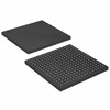
EP3C5F256C6N
Intel
IC FPGA 182 I/O 256FBGA
LE25ABZ
STMicroelectronics
IC REG LINEAR 2.5V 100MA TO92-3
BAJ2CC0FP-E2
Rohm Semiconductor
IC REG LINEAR 12V 1A TO252-3
SMA5J5.0CAHE3/5A
Vishay General Semiconductor - Diodes Division
TVS DIODE 5VWM 9.2VC DO214AC
T835-600B-TR
STMicroelectronics
TRIAC ALTERNISTOR 600V 8A DPAK
TLC5947DAPR
Texas Instruments
IC LED DRVR LINEAR 30MA 32HTSSOP
DRV10983LIPWPR
Texas Instruments
PROTOTYPE -

MPC8541EPXAJD
Freescale Semiconductor
POWERQUICC RISC MICROPROCESSORS,
SMBJ33A
SMC Diode Solutions
TVS DIODE 33VWM 53.3VC SMB
IXFE48N50Q
IXYS
MOSFET N-CH 500V 41A SOT-227B
ISL28113FHZ-T7A
Renesas Electronics America Inc
IC OPAMP GP 1 CIRCUIT SOT23-5
SI2337DS-T1-E3
Vishay Siliconix
MOSFET P-CH 80V 2.2A SOT23-3
MMBT2222A-7
Diodes Incorporated
TRANS NPN 40V 0.6A SOT23-3
NCP163AMX500TBG
onsemi
IC REG LINEAR 5V 250MA 4XDFN
D2D12
Sensata-Crydom
SSR RELAY SPST-NO 12A 0-200V
LM393DGKR
Rohm Semiconductor
IC COMPARATOR 2 GEN PUR 8MSOP
EPM7192SQC160-10N
Intel
IC CPLD 192MC 10NS 160QFP
AT27C4096-15PC
Microchip Technology
IC EPROM 4MBIT PARALLEL 40DIP
GRM033R61E562MA12D
Murata Electronics
CAP CER 5600PF 25V X5R 0201
DS90LV027ATMX
Texas Instruments
IC DRIVER 2/0 8SOIC
FL4000061
Diodes Incorporated
CRYSTAL 40.0000MHZ 15PF SMD
CS5509-ASZ
Cirrus Logic Inc.
IC ADC 16BIT SIGMA-DELTA 16SOIC
SFP9634
Fairchild Semiconductor
MOSFET P-CH 250V 5A TO220-3
GAL16V8D-25QPN
Lattice Semiconductor Corporation
IC CPLD 8MC 25NS 20DIP
LDC18897M20B-320
Murata Electronics
MULTI-LAY HYBRID COUPLER 0603 -
UNR221000L
Panasonic Electronic Components
TRANS PREBIAS NPN 200MW MINI3
GRM1887U2A5R2DZ01D
Murata Electronics
CAP CER 5.2PF 100V U2J 0603
GRM3166R1H560JZ01D
Murata Electronics
CAP CER 56PF 50V R2H 1206
BCM88660A0KFSBLG
Broadcom Limited
TRAFFIC MGR PACKETPROC
GRM1555C1H5R8CA01D
Murata Electronics
CAP CER 5.8PF 50V C0G/NP0 0402
H11A617A3S
onsemi
OPTOISO 5.3KV TRANSISTOR 4SMD
DS3252N
Analog Devices Inc./Maxim Integrated
IC TELECOM INTERFACE 144CSBGA
C2012X7T2W223K125AA
TDK Corporation
CAP CER 0.022UF 450V X7T 0805
VOD207T
Vishay Semiconductor Opto Division
OPTOISOLATOR 4KV 2CH TRANS 8SOIC
SP206EA-L
MaxLinear, Inc.
IC TRANSCEIVER FULL 4/3 24SSOP
ZL50060GAC
Microchip Technology
IC TELECOM INTERFACE 256BGA
OPA2227U/2K5G4
Texas Instruments
IC OPAMP GP 2 CIRCUIT 8SOIC
UDZSTE-1733B
Rohm Semiconductor
DIODE ZENER 33V 200MW UMD2
BTA08-400CRG
STMicroelectronics
TRIAC 400V 8A TO220AB
DS1258AB-100
Analog Devices Inc./Maxim Integrated
IC NVSRAM 2MBIT PARALLEL 40EDIP
GJM1555C1H6R6BB01D
Murata Electronics
CAP CER 6.6PF 50V C0G/NP0 0402
ADS8328IBRSAR
Texas Instruments
IC ADC 16BIT SAR 16QFN
IW1790-09
Renesas Design Germany GmbH
IC OFFLIN CONV SEC SIDE SR 8SOIC