How the ATMEGA168 Microcontroller Works
The ATMEGA168 is a highly efficient 8-bit microcontroller designed for low power usage, perfect for a range of embedded applications. Running on AVR® RISC architecture, it processes instructions quickly while keeping power consumption low, making it ideal for both small projects and more complex systems. With built-in features like memory storage, communication support, and various power-saving modes, the ATMEGA168 offers flexibility and performance for projects that need reliable and responsive control. Whether you are working on robotics, automation, or educational projects, this microcontroller delivers a powerful and versatile solution.Catalog
Overview of the ATMEGA168
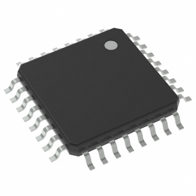
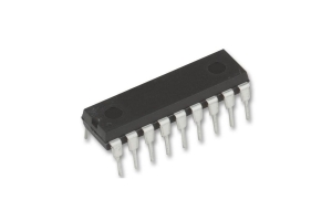
The ATMEGA168 is an 8-bit microcontroller that uses CMOS technology and is designed for low power consumption. It operates on the AVR® RISC architecture, which allows it to execute instructions in a single clock cycle. This design helps optimize power efficiency while maintaining processing speed, enabling the device to process up to one million instructions per second per megahertz. The microcontroller is available in three package types: PDIP, MLF, and TQFP. The PDIP and MLF packages come with 28 pins, while the TQFP package includes 32 pins.
The ATMEGA168 has 16KB of Flash memory for storing programs, 1KB of RAM, and 512 bytes of EEPROM, which ensures long-term data retention of around 20 years. It also includes an onboard 10-bit ADC module, which provides 8 channels for converting analog signals into digital ones—useful for sensor interfaces.
One of the standout aspects of the ATMEGA168 is that it supports SPI, I2C, and USART communication protocols, making it flexible in terms of device-to-device communication. This feature makes it a versatile choice for projects that require communication with multiple external components.
Other useful features include a watchdog timer, power-up timer, oscillator start-up timer, and Brown-out Detection. These built-in features help ensure that your system runs smoothly without unexpected interruptions.
The ATMEGA168 differs from other microcontrollers like the PIC series because it performs most instructions in one clock cycle, whereas PIC microcontrollers may take multiple cycles for similar tasks. Additionally, the AVR microcontroller comes with 32 general-purpose registers, unlike the PIC’s 'W' register. This helps speed up processing tasks and enhances flexibility in programming.
Pinout of the ATMEGA168

ATMEGA168 CAD Design
ATMEGA168 Symbol

ATMEGA168 Footprint

ATMEGA168 3D Model

Key Features of the ATMEGA168
High Performance, Low Power AVR® 8-Bit Microcontroller Family
The ATMEGA168 belongs to a family of microcontrollers designed to offer high performance while consuming minimal power. This balance allows you to use it in applications where both efficiency and processing power are needed without sacrificing battery life or energy usage.
Advanced RISC Architecture
• 131 Instructions: With 131 instructions available, most of which can be executed in a single clock cycle, the ATMEGA168 provides a responsive experience, making your system faster.
• 32 x 8 Working Registers: You can take advantage of 32 general-purpose registers, allowing you to store and process data more effectively within your programs.
• 20 MIPS Throughput: At 20MHz, the ATMEGA168 can deliver up to 20 million instructions per second, giving you plenty of speed for your tasks.
• On-Chip 2-Cycle Multiplier: This feature helps you perform multiplications more quickly, improving processing in complex calculations.
Non-Volatile Memory Segments
• Flash Memory: You can choose from 4KB, 8KB, 16KB, or 32KB of Flash memory, depending on your application needs. This allows for in-system programming, so you can update the microcontroller's software without removing it from the circuit.
• EEPROM: With 512 bytes to 1KB of EEPROM, you can store small amounts of data like calibration values, configurations, or other settings that need to persist between power cycles.
• SRAM: The internal SRAM, ranging from 512 bytes to 2KB, is available for fast data storage during your program's execution.
Memory Retention and Longevity
• Write/Erase Cycles: The Flash memory supports up to 10,000 write/erase cycles, and the EEPROM supports 100,000 cycles, giving you durability in data storage.
• Data Retention: Data stored in EEPROM can last for up to 20 years at 85°C or 100 years at 25°C, making it reliable for long-term applications.
QTouch® Library Support
• Capacitive Touch: The ATMEGA168 supports touch sensors such as buttons, sliders, and wheels, allowing you to integrate touch input into your projects.
• Sense Channels: You can have up to 64 touch sense channels, making it possible to create complex touch interfaces for different applications.
Peripheral Features
• Timer/Counters: It includes two 8-bit timers and one 16-bit timer, giving you flexibility in managing timed tasks or generating precise delays.
• PWM Channels: There are six PWM (Pulse Width Modulation) channels, useful for applications such as motor control or dimming LEDs.
• ADC Channels: The microcontroller comes with a 10-bit ADC (Analog-to-Digital Converter) with 8 channels in TQFP and QFN/MLF packages or 6 channels in PDIP packages. This is perfect for interfacing with sensors.
• Serial Communication: You can use various communication protocols such as USART, SPI, and I2C, allowing easy communication with other devices.
• Watchdog Timer: This feature helps ensure system reliability by resetting the microcontroller if it stops responding.
Special Microcontroller Features
• Power-On Reset and Brown-Out Detection: These features ensure that your system starts correctly after a power cycle and that it can handle low-voltage conditions safely.
• Sleep Modes: The ATMEGA168 offers six sleep modes, including Idle, Power-save, and Standby. This lets you reduce power consumption when full performance isn’t needed, saving battery life.
I/O and Package Options
• Programmable I/O Lines: With 23 programmable input/output lines, you can easily connect various sensors, buttons, or other peripherals to your system.
• Multiple Package Options: The ATMEGA168 is available in several packages, such as 28-pin PDIP and 32-lead TQFP, allowing you to select the most suitable package for your project.
ATMEGA168 Technical Specifications
Microchip Technology ATMEGA168A-AU technical specifications, attributes, parameters, and parts with similar specifications to Microchip Technology ATMEGA168A-AU.
| Type | Parameter |
| Factory Lead Time | 8 Weeks |
| Contact Plating | Tin |
| Mount | Surface Mount |
| Mounting Type | Surface Mount |
| Package / Case | 32-TQFP |
| Number of Pins | 32 |
| Data Converters | A/D 8x10b |
| Number of I/Os | 23 |
| Watchdog Timers | Yes |
| Operating Temperature | -40°C~85°C TA |
| Packaging | Tray |
| Series | AVR® ATmega |
| Published | 1997 |
| JESD-609 Code | e3 |
| Pbfree Code | yes |
| Part Status | Active |
| Moisture Sensitivity Level (MSL) | 3 (168 Hours) |
| Number of Terminations | 32 |
| Terminal Position | QUAD |
| Terminal Form | GULL WING |
| Peak Reflow Temperature (°C) | 260 |
| Supply Voltage | 5V |
| Frequency | 20MHz |
| Time @ Peak Reflow Temperature (Max) | 40s |
| Base Part Number | ATMEGA168A |
| Supply Voltage-Max (Vsup) | 5.5V |
| Power Supplies | 2/5V |
| Supply Voltage-Min (Vsup) | 4.5V |
| Interface | 2-Wire, I2C, SPI, Serial, UART, USART |
| Memory Size | 16kB |
| Oscillator Type | Internal |
| RAM Size | 1K x 8 |
| Voltage - Supply (Vcc/Vdd) | 1.8V~5.5V |
| uPs/uCs/Peripheral ICs Type | MICROCONTROLLER, RISC |
| Core Processor | AVR |
| Peripherals | Brown-out Detect/Reset, POR, PWM, WDT |
| Program Memory Type | FLASH |
| Core Size | 8-Bit |
| Program Memory Size | 16KB 8K x 16 |
| Connectivity | I2C, SPI, UART/USART |
| Bit Size | 8 |
| Has ADC | YES |
| DMA Channels | NO |
| Data Bus Width | 8b |
| Number of Timers/Counters | 3 |
| EEPROM Size | 512 x 8 |
| Boundary Scan | NO |
| Low Power Mode | NO |
| Format | FIXED-POINT |
| Integrated Cache | NO |
| Number of ADC Channels | 8 |
| Number of Serial I/Os | 1 |
| Number of External Interrupts | 2 |
| Number of PWM Channels | 6 |
| Number of I2C Channels | 1 |
| Height | 1.05mm |
| Length | 7mm |
| Width | 7mm |
| REACH SVHC | No SVHC |
| Radiation Hardening | No |
| RoHS Status | ROHS3 Compliant |
| Lead Free | Lead Free |
Comparable Parts to ATMEGA168
The three parts listed on the right have specifications similar to those of the Microchip Technology ATMEGA168A-AU.
| Part Number | ATMEGA168A-AU | ATMEGA88PA-AU | ATMEGA48A-AU | ATMEGA88A-AU |
| Manufacturer | Microchip Technology | Microchip Technology | Microchip Technology | Microchip Technology |
| Package / Case | 32-TQFP | 32-TQFP | 32-TQFP | 32-TQFP |
| Number of Pins | 32 | 32 | 32 | 32 |
| Data Bus Width | 8 b | 8 b | 8 b | 8 b |
| Number of I/O | 23 | 23 | 23 | 23 |
| Interface | 2-Wire, I2C, SPI, Serial, UART | I2C, SPI, Serial, UART, USART | 2-Wire, I2C, SPI, Serial, UART | I2C, SPI, USART |
| Memory Size | 16 kB | 4 kB | 8 kB | 8 kB |
| Supply Voltage | 5 V | 5 V | 5 V | 5 V |
| Peripherals | Brown-out Detect/Reset | Brown-out Detect/Reset | Brown-out Detect/Reset | Brown-out Detect/Reset |
| View Compare | ATMEGA168A-AU vs ATMEGA88PA-AU | ATMEGA168A-AU vs ATMEGA88PA-AU | ATMEGA168A-AU vs ATMEGA48A-AU | ATMEGA168A-AU vs ATMEG |
Functional Block Diagram of the ATMEGA168

The AVR core of the ATMEGA168 is designed with 32 general-purpose registers, which interact directly with the Arithmetic Logic Unit (ALU). This setup allows two independent registers to be accessed simultaneously, completing instructions in just one clock cycle. This efficiency makes the ATMEGA168 far more efficient compared to traditional CISC microcontrollers, delivering processing speeds up to ten times faster.
The ATMEGA168 provides up to 8Kbytes of in-system programmable Flash memory, 1Kbytes of SRAM, and 1Kbytes of EEPROM. It also comes with 23 general-purpose I/O lines, three timer/counters, and a range of communication interfaces, such as USART, SPI, and I2C. Additionally, the microcontroller includes a 6-channel, 10-bit ADC for tasks that require analog-to-digital conversion.
The device supports various power-saving modes to optimize performance and extend battery life. In Idle mode, the CPU is turned off while keeping the peripherals like timers and communication interfaces active. Power-down mode shuts down all functions except for the asynchronous timer, which allows minimal power consumption. Power-save mode keeps the timer active while putting the rest of the device into sleep, and ADC Noise Reduction mode reduces noise during analog-to-digital conversions by turning off unnecessary components. Standby mode offers fast start-up while keeping power consumption low by allowing the oscillator to run while the rest of the system sleeps.
With support for Read-While-Write, you can update the Application Flash memory without interrupting the Boot Flash operations. This allows for continuous operation while reprogramming the memory, making the ATMEGA168 a solid choice for embedded control systems.
Comparison: ATMEGA168 vs. ATMEGA328
The primary distinction between the ATMEGA168 and the ATMEGA328 is the amount of available Flash memory. The ATMEGA168 has 16KB of Flash memory, while the ATMEGA328 offers 32KB, which is ideal if you’re working on larger projects that require more storage space for program data. However, for most hobbyist applications, this difference might not be significant. Both microcontrollers share similar features, pin configurations, and performance characteristics, making them interchangeable in many cases.
If your project requires more memory to store a larger codebase or more extensive data handling, you might opt for the ATMEGA328. Otherwise, for smaller applications or when memory constraints are not an issue, the ATMEGA168 will perform just as well.
Alternatives to the ATMEGA168
| Part Number | Description | Manufacturer |
| ATMEGA168-24AI MICROCONTROLLERS AND PROCESSORS | RISC Microcontroller, 8-Bit, FLASH, 24MHz, CMOS, PQFP32, 7 x 7 MM, 1 MM HEIGHT, 0.80 MM PITCH, PLASTIC, MS-026ABA, TQFP-32 | Atmel Corporation |
Applications of the ATMEGA168
Student Projects
The ATMEGA168 is a great choice for educational projects. Its ease of use and extensive features make it suitable for a variety of small-scale applications, from simple control systems to learning how to interface sensors and motors.
Embedded and Robotics Systems
If you’re working on embedded systems or robotics, the ATMEGA168 offers all the key components you need. Its efficient architecture and the ability to handle communication protocols like SPI and I2C make it an excellent choice for controlling robotic arms, sensors, or autonomous vehicles.
Industrial Automation
In industrial automation, the ATMEGA168 is often used to control machinery or processes. Its timers, ADCs, and communication interfaces allow you to build systems that automate repetitive tasks or control devices in manufacturing environments.
Home Security Systems
The microcontroller is ideal for home security systems, where it can be used to interface with sensors, detect intrusions, or control door locks. With its low power consumption, it’s perfect for battery-powered devices that need to run reliably over long periods.
Designing Quadcopters
If you’re into drone design, the ATMEGA168 can be the brain of your quadcopter. It can handle motor control using PWM channels, process sensor data with its ADCs, and communicate wirelessly with other devices, making it a good option for lightweight, efficient quadcopters.
Packaging of ATMEGA168

Manufacturer Information for ATMEGA168
Microchip Technology Inc. is the company behind the ATMEGA168. Known for producing reliable and cost-efficient microcontroller and analog semiconductor solutions, Microchip’s headquarters are located in Chandler, Arizona. Their focus is on providing products that reduce development risks, lower overall system costs, and help speed up the time to market for various industries.
Datasheet PDF
ATMEGA168A-AU Datasheet:
ATMEGA88PA-AU Datasheet:
ATMEGA48A-AU Datasheet:
ATMEGA88A-AU Datasheet:
Frequently Asked Questions [FAQ]
1. What tools do I need for developing with the ATMEGA168?
The ATMEGA168 offers a full set of tools to make your development easier. These include C language compilers, macro assemblers, program debuggers and simulators, in-circuit emulators, and evaluation boards. These tools help you program, debug, and test your system efficiently. The microcontroller itself comes with 16KB of in-system programmable Flash, 512 bytes of EEPROM, 1K of SRAM, 23 general-purpose I/O lines, and multiple communication interfaces like USART, SPI, and an 8-channel 10-bit ADC.
2. Which one is better: ATMEGA8, ATMEGA48, ATMEGA88, or ATMEGA168?
The ATMEGA48, ATMEGA88, and ATMEGA168 differ mainly in memory size, boot loader support, and how they handle interrupts. The ATMEGA88 and ATMEGA168 support simultaneous read and write operations through an independent Boot Loader area, whereas the ATMEGA48 does not. The ATMEGA8, on the other hand, lacks some interrupt functions and has a smaller memory size. All four chips share the same pin configuration, so you can easily upgrade between them as long as the package is the same.
3. What is the ATMEGA168V-10PU?
The ATMEGA168V-10PU is a variation of the ATMEGA168 microcontroller, designed to operate at lower voltages. It is often used in systems where low power consumption is a priority, making it a great choice for battery-powered applications.
About us
ALLELCO LIMITED
Read more
Quick inquiry
Please send an inquiry, we will respond immediately.
A Comprehensive Overview of the TDA1517P Audio Amplifier
on October 21th
2N3055 Transistor Explained: Features and Uses
on October 21th
Popular Posts
-

Complex Instruction Set Computers: How They Changed Computing?
on April 18th 147749
-

USB-C Pinout and Features
on April 18th 111904
-

Using Xilinx Unified Simulation Primitives: A Comprehensive Guide to FPGA Design and Simulation
on April 18th 111349
-

Power Supply Voltages in Electronics: Meaning of VCC, VDD, VEE, VSS, and GND
on April 18th 83714
-

RJ45 Connector Guide: Pinout, Wiring, Cable Types, and Uses
on January 1th 79502
-

The Ultimate Guide to Wire Color Codes in Modern Electrical Systems
The way our electrical systems use colors isn’t just for looks. Each wire color now indicates a specific function, making it easier to identify and handle electrical components correctly during ins...on January 1th 66868
-

Quality (Q) Factor: Equations and Applications
The quality factor, or 'Q', is important when checking how well inductors and resonators work in electronic systems that use radio frequencies (RF). 'Q' measures how well a circuit minimizes energy...on January 1th 63004
-

Purge Valve Guide: Function, Symptoms, Testing, and Replacement for Optimal Engine Performance
The purge valve is a key part of a car’s system that helps keep the air clean by managing fuel vapors before they can escape into the atmosphere. This not only helps the environment by reducing pol...on January 1th 62937
-

Achieving Peak Performance with the Maximum Power Transfer Theorem
The Maximum Power Transfer Theorem explains how energy from a source, such as a battery or generator, flows to a connected load. It shows the exact condition where the load receives the most power....on January 1th 54076
-

A23 Battery Specifications and Compatibility
The A23 battery is a small, cylinder-shaped battery with high voltage. Also called 23A, 23AE, or MN21, it runs at 12 volts and much higher than AA or AAA batteries. Its special design make...on January 1th 52087
HOT Part Number
-
LTC4063EDD#TRPBF
Analog Devices Inc.
IC BATT CHG LI-ION 1CELL 10DFN
MIMX8MM1CVTKZAA
NXP USA Inc.
IC MPU I.MX 8M MINI SOLOLITE
APDS-9005-020
Broadcom Limited
SENSOR OPT 500NM AMB 6CHIPLED
06031A820KAT2A
KYOCERA AVX
CAP CER 82PF 100V C0G/NP0 0603
ICM-20602
TDK InvenSense
IMU ACCEL/GYRO/TEMP I2C/SPI LGA
170M4611
Eaton - Bussmann Electrical Division
FUSE SQUARE 350A 700VAC RECT
08053C105JAZ2A
KYOCERA AVX
CAP CER 1UF 25V X7R 0805
EP1C12F324C6N
Intel
IC FPGA 249 I/O 324FBGA
2SC4617T1G
onsemi
TRANS NPN 50V 0.1A SC75 SOT416
TL431AILPRAG
onsemi
IC VREF SHUNT ADJ 1% TO92-3
ADAU1787BCBZRL
Analog Devices Inc.
4 ADC, 2 DAC LOW POWER CODEC, AU
74VHC164MTCX
onsemi
IC SHIFT REGISTER 8BIT 14TSSOP
DAN222M3T5G
onsemi
DIODE ARRAY GP 80V 100MA SOT723
NR3015T470M
Taiyo Yuden
FIXED IND 47UH 300MA 1.608OHM SM
MM3Z18VC
onsemi
DIODE ZENER 18V 200MW SOD323F
1N4001W
Rectron USA
DIODE GEN 1A 50V SOD-123F
SMBJ90A
Taiwan Semiconductor Corporation
TVS DIODE 90VWM 146VC DO214AA
NTA1215MC
Murata Power Solutions Inc.
DC DC CONVERTER +/-15V 1W -
SDR1307-101KL
Bourns Inc.
FIXED IND 100UH 1.9A 180MOHM SMD
AOT5B65M1
Alpha & Omega Semiconductor Inc.
IGBT 650V 5A TO220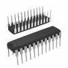
STP16CP596B1R
STMicroelectronics
IC LED DRIVER LINEAR 50MA 24DIP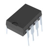
AD7895ANZ-2
Analog Devices Inc.
IC ADC 12BIT SAR 8DIP
MURB1620CTT4G
onsemi
DIODE ARRAY GP 200V 8A D2PAK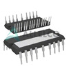
STGIPS30C60T-H
STMicroelectronics
MOD IPM SLLIMM 30A 600V 25SDIP
IXDN604SIA
IXYS Integrated Circuits Division
IC GATE DRVR LOW-SIDE 8SOIC
CY7C63743-SC
Infineon Technologies
IC MCU 8K LS USB/PS-2 24-SOIC
U2745B-MFBG3
Microchip Technology
RF TX IC UHF 310-440MHZ 16LSSOP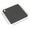
DSPIC30F4013T-30I/PT
Microchip Technology
IC MCU 16BIT 48KB FLASH 44TQFP
ADF4106BRUZ-RL
Analog Devices Inc.
IC CLK/FREQ SYNTH 16TSSOP
EL8403IS
Elantec
IC OPAMP GP 4 CIRCUIT 14SOIC
8A35001B-001AJG
Renesas Electronics America Inc
NETWORK TIMING
GRM0337U1HR90BD01D
Murata Electronics
CAP CER 0.9PF 50V U2J 0201
LT1356CS#PBF
Analog Devices Inc.
IC VOLTAGE FEEDBACK 2 CIRC 16SO
AON7280
Alpha & Omega Semiconductor Inc.
MOSFET N-CH 80V 20A/50A 8DFN
IRLI540N
Infineon Technologies
MOSFET N-CH 100V 23A TO220AB FP
VI-J6Z-MZ
Vicor Corporation
VI-J6Z-MZ 300V 2V 5A -
LMH6722MA
Texas Instruments
IC AMP CURRENT FEEDBACK 14SOIC
HZM6.8Z4MWATL-E
Renesas Electronics America Inc
TVS DIODE 3.5VWM 3MPAK
LM4041DIM7-1.2
Texas Instruments
IC VREF SHUNT 1% SC70-5
RT6200GE
Richtek USA Inc.
IC REG BUCK ADJ 600MA SOT23-6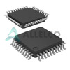
R5F21274SNFP#X6
Renesas Electronics America Inc
IC MCU 16BIT 16KB FLASH 32LQFP
1N5227B
onsemi
DIODE ZENER 3.6V 500MW DO35
12102C472JAT2A
KYOCERA AVX
CAP CER 4700PF 200V X7R 1210
PZTA64
Fairchild Semiconductor
SMALL SIGNAL BIPOLAR TRANSISTOR,
XC1765ELSO8C
AMD
IC PROM SER C-TEMP 3.3V 8-SOIC
XR88C92CJ-F
MaxLinear, Inc.
IC UART FIFO DUAL 44PLCC
RT24C2X202
Bourns, Inc.
TRIMMER 2K OHM 0.75W PC PIN SIDE
DLW31SN900SQ2L
Murata Electronics
CMC 370MA 2LN 90 OHM SMD
LMK432F476ZM-T
Taiyo Yuden
CAP CER 47UF 10V Y5V 1812
MOC207R1VM
onsemi
OPTOISO 2.5KV TRANS W/BASE 8SOIC
GRM0335C1E390JD01D
Murata Electronics
CAP CER 39PF 25V C0G/NP0 0201
SE10PG-M3/84A
Vishay General Semiconductor - Diodes Division
DIODE GEN PURP 400V 1A DO220AA
RABS15M REG
Taiwan Semiconductor Corporation
BRIDGE RECT 1P 1KV 1.5A ABS-L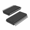
PI74LPT16245AEX
Diodes Incorporated
IC TXRX NON-INVERT 3.6V 48TSSOP