
Understanding Gated SR Latches: Truth Table, Circuits and Working Principle
A gated SR latch is a simple circuit that stores one bit of data. It works only when an enable or clock signal is on, making it more reliable than a basic SR latch. This article explains how it works, how it is built with logic gates, its symbol and truth table, its timing, its use in PLCs, how it differs from a basic SR latch, where it is used, and its pros and cons.Catalog

Figure 1. Gated SR Latch
What is a Gated SR Latch?
A gated SR latch, also called a clocked or synchronous SR latch, is an improved version of the basic SR latch that includes an enable signal (or clock/control input). The output changes only when this enable signal is active, allowing updates to occur in a controlled and timed manner.
This design prevents the unpredictable behavior often seen in simple SR latches, which react immediately to input changes without timing control. By using the enable signal as a gate, the latch synchronizes both data storage and retrieval.
Gated SR Latch Circuits
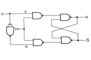
Gated SR Latch Using NOR and AND Gates

Figure 2. Gated SR Latch Using NOR and AND Gates
This design stores one bit of data using a combination of AND and NOR gates. The circuit includes three inputs: Set (S), Reset (R), and Clock (Clk). It produces two complementary outputs, Q and Q̅, representing the stored value and its inverse.
The AND gates act as filters. They allow the Set and Reset inputs to reach the NOR-based memory core only when Clk is high (logic 1). When Clk is low, the AND gates block any changes, and the latch holds its previous state.
The cross-coupled NOR gates form a feedback loop, which is the core memory element. This loop ensures that the circuit “remembers” its current state until a new valid input overrides it.
Operation of NOR-AND Latch:
• Set condition: S = 1, R = 0, Clk = 1 → Q is forced to 1 (latch stores a high).
• Reset condition: R = 1, S = 0, Clk = 1 → Q is forced to 0 (latch stores a low).
• Hold condition: S = 0, R = 0, Clk = 1 → Q keeps its previous value (no change).
• Invalid condition: S = 1, R = 1 → Q enters an undefined state (must be avoided).
Gated SR Latch Using NAND Gates

Figure 3. Gated SR Latch Using NAND Gates
A NAND-based gated SR latch works on the same principle but replaces NOR logic with NAND logic. It still has S, R, and Clk inputs and produces complementary outputs Q and Q̅.
The NAND gates ensure that Set and Reset can modify the state only when Clk is active (high). The cross-coupled NAND gates then lock the output into its last state, similar to the NOR version.
Operation of NAND-Based Latch:
• Set condition: S = 1, R = 0, Clk = 1 → Q = 1.
• Reset condition: R = 1, S = 0, Clk = 1 → Q = 0.
• Hold condition: S = 0, R = 0, Clk = 1 → Q retains its current state.
• Invalid condition: S = 1, R = 1 → Q becomes undefined.
Symbol of a Gated SR Latch

Figure 4. Symbol of a Gated SR Latch
The symbol for a gated SR latch shows three inputs: Set (S), Reset (R), and Enable (E), and two outputs, Q and Q̅. The behavior is simple. When E is high, the latch responds to S and R inputs. When E is low, the latch ignores input changes and keeps its current output.
Gated SR Latch Truth Table
|
Enable (E) |
Set (S) |
Reset (R) |
Next Q |
Description |
|
0 |
X |
X |
Q |
Latch disabled |
|
1 |
0 |
0 |
Q |
Hold state |
|
1 |
1 |
0 |
1 |
Set state |
|
1 |
0 |
1 |
0 |
Reset state |
|
1 |
1 |
1 |
– |
Undefined state |
When E = 0, the latch does nothing. Q simply holds whatever value it had before.
Timing Diagram of a Gated SR Latch
Figure 5. Timing Diagram of a Gated SR Latch
A timing diagram illustrates how a latch or flip-flop responds to its input signals (in this case, S, R, and Clk) over time. For a Gated SR Latch, the clock signal (Clk) controls when the outputs Q and Qˉ are allowed to change.
1. At t1:
The clock signal Clk = 1, and the set input S = 0. With R = 1 (reset active), the latch is reset, and Q = 0 while Qˉ=1.
2. At t2:
S switches to 1 while Clk is still 1. This activates the set condition, causing Q to switch to 1 and Qˉ to 0.
3. At t3:
The clock drops to 0. At this point, the latch is “frozen,” meaning Q and Qˉ hold their current values regardless of changes in S or R. The gated latch updates outputs only when Clk = 1.
4. At t4:
Clk rises back to 1, and the outputs Q and Qˉ again respond to the current states of S and R. For example, if R = 1 and S = 0, Q will reset to 0.
Gated SR Latch in Ladder Logic
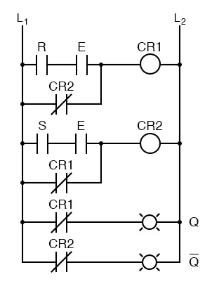
Figure 6. Gated SR Latch in Ladder Logic
In programmable logic controllers (PLCs), latching circuits are important for memory functions. A gated SR latch can be implemented using ladder logic diagrams, as shown above.
In this circuit:
• CR1 acts as the Set relay (S).
When both Enable (E) and S are active (logic high), CR1 energizes, setting the output Q to high (1).
• CR2 acts as the Reset relay (R).
When both E and R are active, CR2 energizes, which resets Q to low (0).
• Enable (E) acts as a gate signal, ensuring that the latch responds to S or R only when E is high.
When E is low, no state change occurs, and Q retains its previous state (it "latches").
Difference Between Gated SR Latch and Basic SR Latch
|
Aspect |
Basic SR
Latch |
Gated SR
Latch |
|
Control Signal |
No Enable input; directly controlled by S and R. |
Includes an Enable (E) input to control operation. |
|
Response |
Output changes immediately with S or R input. |
Output changes only when Enable (E) is active. |
|
Synchronization |
Operates asynchronously. |
Operates synchronously with Enable signal. |
|
Timing Control |
No specific timing control. |
Timing is regulated by Enable or clock signals. |
|
Glitch Prevention |
Susceptible to unwanted state changes. |
Reduces glitches by requiring Enable to be high. |
|
Design Complexity |
Simple structure with just NOR or NAND gates. |
Slightly more complex due to additional control input. |
|
Output Stability |
Output may change unexpectedly when inputs vary. |
Output remains stable when Enable is low. |
|
Suitability for Flip-Flops |
Not ideal for clocked flip-flop design. |
Used as a basis for creating clocked flip-flops. |
|
Applications |
Small logic circuits and simple memory storage. |
Sequential logic, memory units, and clocked systems. |
|
Power Consumption |
Slightly lower due to fewer gates. |
Slightly higher due to the additional control logic. |
Gated SR Latch Advantages and Limitations
Advantages
• Controlled and predictable state changes, making it reliable for binary storage.
• Simple design that requires only a few basic logic gates.
• Easily integrates with synchronous circuits as a building block.
• Low hardware cost due to minimal gate requirements.
• Fast response time because outputs change quickly with inputs (limited by gate delay).
• Serves as the foundation for building flip-flops, registers, and memory systems.
• Easy to understand conceptually, making it ideal for learning about sequential circuits.
Limitations
• Undefined or invalid behavior when both S and R inputs are high.
• Sensitive to input glitches or noise due to level-triggered nature.
• Requires additional logic in complex designs to prevent invalid input conditions.
• Less reliable for precise timing in high-speed systems compared to edge-triggered flip-flops.
• Limited functionality on its own, cannot store more than one bit without additional components.
• Risk of race conditions if inputs change simultaneously or very close together.
Conclusion
A gated SR latch is an important part of digital circuits because it stores data in a safe and controlled way. It is useful for avoiding glitches, matching signals with clock timing, and building more complex circuits like flip-flops and memory units. Its design is simple and works well for tasks like holding data, cleaning signals, and keeping control signals active. However, it can have problems if both set and reset inputs are active at the same time, and it can be sensitive to noise. It also stores only one bit of data, so it needs extra parts for bigger or faster systems.
About us
ALLELCO LIMITED
Read more
Quick inquiry
Please send an inquiry, we will respond immediately.
Frequently Asked Questions [FAQ]
1. Can I use a gated SR latch for building custom flip-flops or registers?
Yes, gated SR latches are the basic parts used to create more advanced flip-flops like D or JK flip-flops. They can also be combined with other logic parts to make registers, counters, and small memory units. Their simple design makes them great for testing ideas and learning.
2. How do I choose between a NOR-based or NAND-based gated SR latch?
Both NOR- and NAND-based designs function similarly but use different logic gates. A NOR-based design is easier to understand conceptually, while a NAND-based latch might be preferred in certain circuit designs where NAND logic is more efficient or readily available.
3. Do gated SR latches consume a lot of power?
No, gated SR latches are generally low-power components because they use only a few logic gates. However, the power consumption may vary slightly depending on whether you use NOR or NAND designs and the number of latches integrated into your circuit.
4. Are gated SR latches easy to integrate into modern digital systems?
Yes, gated SR latches are easy to integrate due to their simple gate-based design and compatibility with standard logic families like TTL or CMOS. They are often used as building blocks for more complex storage and synchronization circuits.
5. Can gated SR latches be used for long-term data storage?
No, gated SR latches are designed for short-term, volatile data storage. They hold data as long as the circuit is powered and the enable signal controls updates. For long-term storage, non-volatile memory devices like flash memory or EEPROM are recommended.
A guide to the basics of D flip-flops - circuits, truth tables, types, advantages and limitations
on May 17th
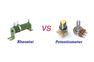
Comparative Guide to Analyzing rheostat and Potentiometers
on May 17th
Popular Posts
-

Complex Instruction Set Computers: How They Changed Computing?
on June 14th 148402
-

USB-C Pinout and Features
on June 14th 131612
-

Using Xilinx Unified Simulation Primitives: A Comprehensive Guide to FPGA Design and Simulation
on June 14th 111884
-

Power Supply Voltages in Electronics: Meaning of VCC, VDD, VEE, VSS, and GND
on June 14th 94454
-

RJ45 Connector Guide: Pinout, Wiring, Cable Types, and Uses
on January 1th 93987
-

The Ultimate Guide to Wire Color Codes in Modern Electrical Systems
The way our electrical systems use colors isn’t just for looks. Each wire color now indicates a specific function, making it easier to identify and handle electrical components correctly during ins...on January 1th 76891
-

Quality (Q) Factor: Equations and Applications
The quality factor, or 'Q', is important when checking how well inductors and resonators work in electronic systems that use radio frequencies (RF). 'Q' measures how well a circuit minimizes energy...on January 1th 74843
-

Purge Valve Guide: Function, Symptoms, Testing, and Replacement for Optimal Engine Performance
The purge valve is a key part of a car’s system that helps keep the air clean by managing fuel vapors before they can escape into the atmosphere. This not only helps the environment by reducing pol...on January 1th 68783
-

Understanding Capacitors and Their Symbols in Circuit Diagrams
Capacitors are small parts used in almost all electronic devices. They store and release electrical energy and are found in things like power supplies, radios, and circuits that help reduce noise. ...on June 14th 58528
-

A23 Battery Specifications and Compatibility
The A23 battery is a small, cylinder-shaped battery with high voltage. Also called 23A, 23AE, or MN21, it runs at 12 volts and much higher than AA or AAA batteries. Its special design make...on January 1th 58132
HOT Part Number
-
MAX3100CEE-T
Analog Devices Inc./Maxim Integrated
IC UART SPI/MICRWIRE COMP 16QSOP
BD9B100MUV-E2
Rohm Semiconductor
IC REG BUCK ADJ 1A 16VQFN
UPD70F3539AF5A9-PN7-Q-A
Renesas Electronics America Inc
IC MICROCONTROLLER
18081A621JAT2A
KYOCERA AVX
CAP CER 620PF 100V NP0 1808
FDN340P
onsemi
MOSFET P-CH 20V 2A SUPERSOT3
70231-101
Amphenol ICC (FCI)
CONN RCPT BLADE PWR 8POS EDGE MT
MPSW42RLRAG
onsemi
TRANS NPN 300V 0.5A TO92
MC7824BT
onsemi
IC REG LINEAR 24V 1A TO220AB
LT1815CS5#TRPBF
Analog Devices Inc.
IC OPAMP VFB 1 CIRCUIT TSOT23-5
DG411DYZ
Renesas Electronics America Inc
IC SWITCH SPST-NCX4 35OHM 16SOIC
VFT2060C-M3/4W
Vishay General Semiconductor - Diodes Division
DIODE SCHOTTKY 20A 60V ITO-220AB
TSX562AIYST
STMicroelectronics
IC CMOS 2 CIRCUIT 8MINISO
MR256D08BMA45
Everspin Technologies Inc.
IC RAM 256KBIT PARALLEL 48FBGA
VSC3312YYP-01
Microchip Technology
IC SWITCH 16X16 6.5GBPS 196FCBGA
XC68HC908GP20CFB
Motorola
TSG 8BIT20K FLASH
CSR8811A08-ICXR-R
Qualcomm
IC RF TXRX+MCU BLUETOOTH
HIN202ECBN
Intersil
IC TRANSCEIVER FULL 2/2 16SOIC
MPSW05
onsemi
TRANS NPN 60V 0.5A TO92 -
12065C102JAZ2A
KYOCERA AVX
CAP CER 1000PF 50V X7R 1206
1N4055R
Solid State Inc.
DIODE GEN PURP REV 900V 275A DO9
ASX342ATSC00XPED0-DP
onsemi
IMAGE SENSOR VGA 1/4 CIS SOC
0433.125NR
Littelfuse Inc.
FUSE BOARD MNT 125MA 125VAC/VDC
1SMA5941BT3G
onsemi
DIODE ZENER 47V 1.5W SMA
DCP010512BP-U/700
Texas Instruments
DC DC CONVERTER 12V 1W
1N2134A
Solid State Inc.
DIODE GEN PURP 350V 70A DO5
1-1734344-1
TE Connectivity AMP Connectors
CONN D-SUB HD RCPT 15P R/A SLDR
KSD1621STF
onsemi
TRANS NPN 25V 2A SOT89-3
BQ24161RGET
Texas Instruments
IC BATT CHG LI-ION 1CELL 24VQFN
BTA26-600BW
STMicroelectronics
TRIAC ALTERNISTOR 600V 25A TOP3
NCP1239DD65R2G
onsemi
IC OFFLINE SWITCH FLYBACK 7SOIC
BQ20Z90DBTR-V150
Texas Instruments
IC GAS GAUGE LI-ION 30TSSOP
PCMB104T-1R0MT
Susumu
FIXED IND 1UH 18A 3.3 MOHM SMD
CY29942AXCT
Infineon Technologies
IC CLK BUFFER 1:18 200MHZ 32TQFP
CC0402KRX7R9BB561
YAGEO
CAP CER 560PF 50V X7R 0402
STPS20M60SG-TR
STMicroelectronics
DIODE SCHOTTKY 60V 20A D2PAK
AT25010N-10SC-2.7
Microchip Technology
IC EEPROM 1KBIT SPI 3MHZ 8SOIC -
04023A1R0CAT4A
KYOCERA AVX
CAP CER 1PF 25V C0G/NP0 0402
ISL6327IRZ
Intersil
SWITCHING CONTROLLER, VOLTAGE-MO
LQW18AN75NG0ZD
Murata Electronics
FIXED IND
DFA100BA160
SanRex Corporation
DIODE MODULE 1600V 100A
BAR46AFILM
STMicroelectronics
DIODE ARRAY SCHOTTKY 100V SOT23
MAX825SEUK
Analog Devices Inc./Maxim Integrated
IC SUPERVISOR MPU
LTC3891IUDC#TRPBF
Analog Devices Inc.
IC REG CTRLR BUCK 20QFN
FODM8801AR2
onsemi
OPTOISO 3.75KV TRANS 4-MINI-FLAT
FJV1845FMTF
Fairchild Semiconductor
SMALL SIGNAL BIPOLAR TRANSISTOR,
KSZ8893FQLI-FX
Microchip Technology
IC SWITCH ETH 3PORT 128QFP
170M6340
Eaton - Bussmann Electrical Division
FUSE SQUARE 400A 1.3KVAC RECT
BCM20741A2KFB1G
Broadcom Limited
SINGLE-CHIP BLUETOOTH
GRM0335C1H9R3DA01D
Murata Electronics
CAP CER 9.3PF 50V C0G/NP0 0201
TNY175PN
Power Integrations
11.5 W (85-265 VAC) 15 W (230 VA
742700726
Würth Elektronik
FERRITE CORE 278 OHM SOLID 4MM
DM74S20N
onsemi
IC GATE NAND 2CH 4-INP 14DIP
P4SMA56CA-E3/61
Vishay General Semiconductor - Diodes Division
TVS DIODE 47.8VWM 77VC DO214AC
GRM1885C1HR80CA01D
Murata Electronics
CAP CER 0.8PF 50V C0G/NP0 0603