Why the IC 741 Op Amp is a Must-Know for Electronics?
The IC 741 operational amplifier is a widely used electronic component designed to amplify and process analog signals. It is known for its flexibility, reliability, and ease of use, making it a go-to choice for various applications like signal amplification, integration, and differentiation. This article covers its features, pin configuration, applications, and working principles in detail.Catalog

Introduction to Operational Amplifiers
Operational amplifiers, or op-amps, are widely used in electronics because of their ability to process analog signals. They are designed to amplify electrical signals and perform operations like addition, subtraction, and integration. You’ll often find op-amps in devices that require precise signal control, such as audio equipment, measuring instruments, and control systems.
One of the reasons op-amps are so versatile is their high voltage gain. This means they can take even very small input signals and amplify them significantly. By adding external components like resistors and capacitors, you can tailor an op-amp to perform a variety of functions, including filtering and comparison.
Op-amps play a big role in circuits that require accuracy and reliability. Among the many types available, the IC 741 is one of the most popular because of its versatility and ease of use. Whether you’re building a simple amplifier or designing more complex systems, the IC 741 provides a reliable foundation.
Overview of IC 741 Op Amp
The IC 741 is a classic operational amplifier known for its versatility and wide range of applications. First introduced in 1963 by Fairchild Semiconductors, it quickly became a standard in the world of analog electronics. This op-amp is designed to amplify input signals and perform mathematical operations, making it suitable for tasks like addition, subtraction, and signal integration.
One of the standout features of the IC 741 is its high voltage gain, which allows it to amplify even weak signals effectively. It also operates reliably over a wide range of supply voltages and includes features like short-circuit protection and internal frequency compensation. These characteristics make it a go-to choice for students, hobbyists, and professionals working on analog circuits.
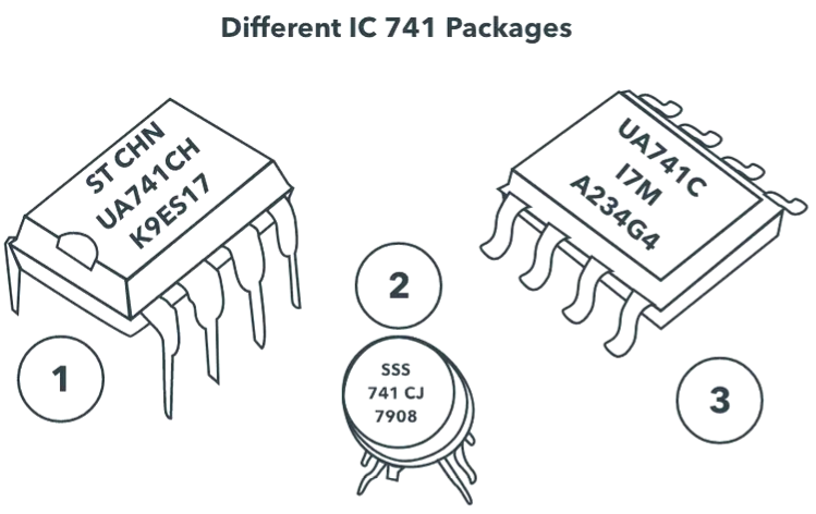
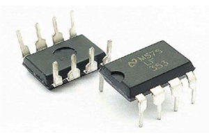
The IC 741 is available in different packages, such as the 8-pin DIP, TO5-8 metal can, and SOIC formats, giving users flexibility in how they integrate it into their designs. Its ease of use and reliability make it a fundamental building block in many electronic projects.
Key Features of IC 741 Op Amp
| Parameter | Value |
| Input Impedance | Greater than 100 kilo-ohms |
| Output Impedance | Less than 100 ohms |
| Frequency Range | 0 Hz to 1 MHz |
| Offset Current/Voltage | Low |
| Voltage Gain | Approximately 200,000 |
Technical Specifications of IC 741
| Parameter | Value |
| Power Supply | Requires a minimum voltage of 5V and can tolerate up to 18V |
| Input Impedance | Approximately 2 MΩ |
| Output Impedance | About 75 Ω |
| Voltage Gain | 200,000 for low frequencies (200 V/mV) |
| Maximum Output Current | 20 mA |
| Recommended Output Load | Greater than 2 KΩ |
| Input Offset | Ranges between 2 mV and 6 mV |
| Slew Rate | 0.5 V/µS (rate at which an Op-Amp detects voltage changes) |
The IC 741's high input impedance and low output impedance make it highly suitable for use as a voltage amplifier.
The table below gives a summary of the standard specifications for the IC 741 operational amplifier.
| Parameter | Symbol | Typical Value | Unit |
| Supply Voltage | Vcc | ±15 | V |
| Output Voltage Swing | Vout | ±14 | V |
| Output Current | Iout | 25 | mA |
| Open-Loop Gain | Aol | 200,000 | V/V |
| Input Impedance | Zin | 2 | MΩ |
| Output Impedance | Zout | 75 | Ω |
| Offset Voltage | Vos | 1 | mV |
| Offset Voltage Drift | TCVos | 7 | µV/°C |
| Offset Voltage Aging | AVos/At | 0.3 | µV/month |
| Slew Rate | SR | 0.5 | V/µs |
| Bandwidth | BW | 1.5 | MHz |
| Common-Mode Rejection Ratio | CMRR | 90 | dB |
| Power Supply Rejection Ratio | PSRR | 86 (positive), 96 (negative) | dB |
IC 741 Op Amp Pin Layout
Understanding IC 741 Pin Configuration
The diagram shows eight pins, with three of them—pins 2, 3, and 6—being particularly meaningful. Pin 2 represents the inverting terminal, while Pin 3 is the non-inverting terminal. These are the input points where signals are applied. Pin 6 serves as the output terminal, delivering the amplified or processed signal.
Pin 8 is not used in the circuit and has no active role. The "741" in the IC's name reflects the design, where seven of the pins are active, including four pins for input (2, 3, 4, and 7) and one for output (6). The triangular shape in the internal diagram of the IC represents its function as an operational amplifier, emphasizing its role in signal processing and amplification tasks.

Explanation of IC 741 Pin Functions
• Power Supply Pins: Pin 4 and Pin 7
Pins 4 and 7 are the power connections for the IC 741. Pin 4 connects to the negative voltage supply, while Pin 7 connects to the positive voltage supply. These pins provide the energy required for the IC to operate. The IC can work within a voltage range of 5V to 18V, which makes it flexible for various circuit designs. Ensuring a stable power supply to these pins is important for the reliable operation of the op-amp.
• Output Pin: Pin 6
Pin 6 is where the output of the IC 741 is available. The voltage at this pin depends on the feedback mechanism and the input voltages at Pin 2 and Pin 3. If the output voltage is high, it will approach the positive supply voltage connected to Pin 7. On the other hand, if the output voltage is low, it will move closer to the negative supply voltage at Pin 4. This pin reflects the amplified or processed signal based on the input and circuit configuration.
• Input Pins: Pin 2 and Pin 3
Pin 2 and Pin 3 are the input terminals for the IC. Pin 2 acts as the inverting input, while Pin 3 serves as the non-inverting input. If the voltage at Pin 2 is higher than at Pin 3, the output voltage will drop low. Conversely, when the voltage at Pin 3 is higher than at Pin 2, the output voltage will rise. These inputs allow you to control the output by varying the input signals, making them central to how the op-amp operates in different configurations.
• Offset Null Pins: Pin 1 and Pin 5
Pin 1 and Pin 5 are used to adjust the offset voltage of the IC 741. Due to small irregularities in the manufacturing process or design, slight voltage differences at the input pins can affect the output. To fix this, an offset voltage can be applied to Pins 1 and 5 using an external potentiometer. This adjustment helps fine-tune the output for greater accuracy in sensitive circuits.
• Not Connected Pin: Pin 8
Pin 8 does not have any internal or external connections in the IC 741. It is simply left unconnected and has no role in the functioning of the IC. This pin occupies the space for structural purposes within the 8-pin package.
Working Principle of IC 741 Op Amp
The IC 741 operates by amplifying the difference between two input signals—one connected to the inverting terminal and the other to the non-inverting terminal. This difference is then processed through a series of internal components, including transistors and current mirrors, which work together to ensure accurate and stable amplification.
The input stage of the IC 741 uses a differential amplifier, which isolates the inputs and prevents unwanted signal feedback. This stage sets the foundation for how the op-amp reacts to different input voltages. The signal then passes through an intermediate stage where it is further processed and amplified. Current mirrors within the IC regulate the flow of current, ensuring consistent performance even with varying input conditions.
Finally, the signal reaches the output stage, where it is prepared for delivery to the connected load. This output can either be in phase with the input (non-inverting mode) or inverted (inverting mode), depending on the circuit configuration. The IC 741 is designed to handle a wide range of input voltages and amplify them with minimal distortion, making it a reliable choice for precise analog signal processing.
Internal Structure of IC 741

The internal structure of the IC 741 is a carefully designed arrangement of transistors, resistors, and current mirrors, all integrated onto a single chip. This design allows the op-amp to handle complex operations with accuracy and stability.
At its core, the IC 741 has a differential input stage, where two transistors process the inverting and non-inverting inputs. This stage determines the difference between the two input signals while ensuring isolation to prevent feedback issues. The output of this stage is then sent to a second amplification stage for further signal boosting.
To regulate current flow and ensure stability, the IC uses current mirrors—special transistor configurations that control and replicate current with precision. These current mirrors help the op-amp maintain consistent performance across a range of operating conditions.
The final output stage includes additional transistors and resistors, which shape the amplified signal for delivery to the output pin. This stage also includes protection mechanisms, such as short-circuit protection, to safeguard the IC during operation.
Overall, the internal structure of the IC 741 is designed to balance high performance with reliability, making it suitable for a wide range of analog applications.
Frequency and Gain Characteristics of IC 741
The IC 741's ability to amplify signals varies depending on the frequency of the input signal. At lower frequencies, typically below 10Hz, the gain remains relatively constant and extremely high, around 200,000. This allows the op-amp to effectively amplify small input signals with minimal distortion.
As the frequency of the input signal increases, the gain gradually decreases. This drop in gain becomes significant as the frequency approaches 100,000Hz, where the gain eventually reduces to unity (1). This behavior is typical of operational amplifiers and is influenced by internal limitations, such as capacitance and bandwidth.
This relationship between gain and frequency is depicted in the graph below, showing how the IC 741 transitions from high gain at low frequencies to much lower gain at higher frequencies.
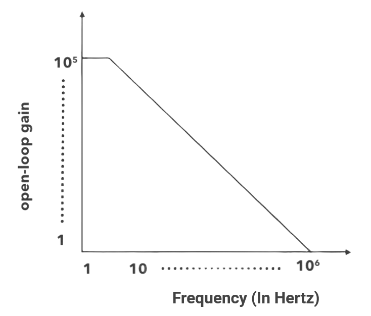
Understanding this characteristic is crucial for designing circuits that require precise control of signal amplification across different frequencies. It helps in selecting the right configurations and components to achieve the desired performance.
IC 741 as an Integrator and Differentiator
The IC 741 can be configured as an integrator or differentiator, allowing it to perform mathematical operations on analog signals. These configurations require specific components and connections to shape the output signal based on the input.
To explore these roles, you'll need a breadboard, resistors, capacitors, an IC 741, a regulated power supply, and an oscilloscope (CRO). The integrator and differentiator circuits are detailed below.
IC 741 as an Integrator

The integrator circuit, built using the IC 741, generates an output that corresponds to the integral of the input signal. This means the output represents the cumulative value of the input over time. Setting up the circuit is straightforward and allows you to see how the IC 741 processes signals.
To begin, apply a sine wave input signal with a frequency of 1 kHz and an amplitude of 2V peak-to-peak. This input signal drives the circuit and serves as the basis for observing the integrator's performance. Once the circuit is set, connect the input and output sections to the channels of a CRO (Cathode Ray Oscilloscope). This setup lets you view and compare the waveforms.
By observing the waveforms on the CRO, you can clearly see how the IC 741 converts the input signal into an integrated output. Take note of the waveforms and compare them with theoretical predictions to confirm the circuit's behavior. This process highlights the IC 741’s ability to perform mathematical operations like integration, which is widely used in analog signal processing.
IC 741 as a Differentiator
The differentiator circuit using the IC 741 is designed to produce an output that represents the rate of change of the input signal. This means it highlights how quickly the input signal changes over time, making it useful for applications that require detecting changes or transitions in signals.
To set up this circuit, apply a triangular wave signal with a frequency of 1 kHz and an amplitude of 2V peak-to-peak to the input. This input waveform allows you to observe how the circuit responds to varying rates of change in the signal.
Next, connect the input and output sections of the circuit to the CRO (Cathode Ray Oscilloscope) channels. This step enables you to monitor and analyze the waveforms in real-time. As you observe the output waveform on the CRO, compare it to the theoretical expectations to verify how well the differentiator circuit performs.
This configuration demonstrates the IC 741’s capability to calculate the derivative of input signals, making it an essential tool for signal processing tasks requiring precision.

Both configurations showcase how flexible the IC 741 is in handling mathematical operations on signals. The ability to act as an integrator or differentiator makes it a valuable component in signal processing, control systems, and various electronic instrumentation applications. This versatility highlights its usefulness in circuits that require precision and adaptability.
Open-Loop Applications of IC 741
In an open-loop setup, the IC 741 operates without feedback, allowing it to achieve a maximum voltage gain of up to 200,000. This configuration is ideal for comparator applications, where the op-amp compares the voltage at its inverting and non-inverting inputs, producing either a positive or negative output based on the comparison. However, due to the high sensitivity, open-loop mode is less suited for amplification. For stable and controlled gain, feedback is added, transitioning the op-amp to a closed-loop configuration.
Common Circuit Configurations of IC 741
IC 741 Op Amp Circuit Diagram

The IC 741 operational amplifier can be configured for various applications, including as an adder, subtractor, comparator, voltage follower, integrator, or differentiator. These applications highlight the op-amp's ability to handle mathematical operations and signal processing efficiently.
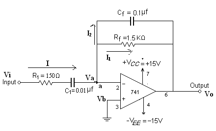
The circuit diagram below demonstrates the IC 741 being used as a comparator. In this setup, the IC identifies and processes weak signals, making it easier to distinguish and analyze them in the circuit.
To further explore its functionality, let’s look at two different voltage amplifier circuits built using the IC 741. These configurations showcase the op-amp’s flexibility and performance in amplifying signals for various uses.
Circuit for inverting amplifier
Inverting Amplifier Circuit Using 741 Op Amp
In an inverting amplifier using the 741 op-amp, Pin 2 serves as the input, while Pin 6 is the output. When the input signal is applied to Pin 2, the output obtained from Pin 6 is reversed in polarity. This means that a positive input results in a negative output, and a negative input results in a positive output. This behavior is why it is called an inverting amplifier.
The circuit diagram and the corresponding input-output waveform are shown below:

The gain of this amplifier is determined using the formula:
Gain (Av) = -(R2 / R1)
The negative sign in the formula indicates the inversion of the output signal's polarity. By changing the values of resistors R1 and R2, you can control how much the input signal is amplified.
Circuit for non-inverting amplifier
In a non-inverting amplifier using the 741 op-amp, Pin 3 is used as the input, and the output is taken from Pin 6. The output maintains the same polarity as the input, meaning that a positive input results in a positive output, while a negative input produces a negative output. This characteristic gives it the name non-inverting amplifier.
The circuit diagram and input-output waveform for the non-inverting amplifier are provided below:

The formula for calculating the gain in this configuration is:
Gain (Av) = 1 + (R2 / R1)
Here, the gain depends on the values of resistors R1 and R2. Adjusting these resistor values allows you to achieve the desired amplification level without reversing the signal's polarity.
Applications of IC 741 Op Amp
The IC 741 operational amplifier is a versatile component widely used in many electronic circuits. Below is an elaboration of its various applications:
Amplifiers
The IC 741 is widely used to amplify signals across different frequencies. It can handle signals from DC to higher radio frequencies, making it suitable for many applications. For instance, you’ll often see it in frequency-selective amplifiers, which are critical in tone control systems for stereo and Hi-Fi audio setups. This ability to selectively amplify specific frequencies helps enhance sound quality in these systems.
Computational Circuits
When it comes to performing mathematical operations, the IC 741 shines. It is commonly used in circuits designed for integration, differentiation, and summing. These operations are valuable in signal processing and control systems where precise mathematical functions are required to manipulate analog signals.
Rectifiers
In applications where regular diodes fall short due to voltage drops, the IC 741 acts as a precision rectifier. It behaves like an ideal diode with no voltage drop, enabling accurate signal rectification. This feature is especially useful in processing weak signals without distortion.
Oscillators
The IC 741 plays an important role in generating oscillations. You'll find it in function generators producing a variety of output waveforms, such as sinusoidal, square, and triangular waves. Additionally, it is often used in Pulse Width Modulators (PWM generators), which are essential in power control circuits.
Comparators
The IC 741 is widely used as a comparator, determining whether two voltages are at the same level. This functionality is useful in applications like voltage regulation and signal comparison circuits. It helps in designing systems that need to make decisions based on voltage thresholds.
Analog-to-Digital and Digital-to-Analog Conversion
The IC 741 contributes to converting digital signals into analog ones and vice versa. It is commonly employed in Digital-to-Analog Converters (DACs) to translate binary input into corresponding analog outputs. Similarly, it is used in Analog-to-Digital Converters (ADCs), enabling smooth interaction between analog and digital systems.
Various Other Applications
• Variable Audio Frequency Oscillator: Helps generate adjustable audio signals for testing and sound production.
• Adjustable Ripple Regulated Power Supply: Ensures a stable power supply by minimizing voltage fluctuations.
• Four-Channel Audio Mixer: Combines audio signals from multiple inputs into one output channel.
• Light-Operated Switch: Works with light-dependent resistors (LDRs) to control devices based on light intensity.
• DC Voltage Polarity Meter: Identifies the polarity of DC voltage in circuits.
• Room Thermometer: Measures room temperature using a sensor circuit.
• Bug Listener: Amplifies sound for listening devices.
• Microphone Amplifier: Increases the strength of microphone signals for audio equipment.
• Op-Amp Tester: Checks the functionality of operational amplifiers.
• Short Circuit Protection for RPS: Prevents damage by safeguarding against short circuits.
• Thermal Touch Switch: Activates devices with a touch-sensitive thermal switch.
• Voltage-to-Frequency Conversion: Converts voltage signals into corresponding frequency outputs.
Conclusion
The IC 741 operational amplifier is a versatile and reliable component widely used in electronic circuits for amplifying signals, performing mathematical operations, and controlling voltage. Its simple design, ease of use, and ability to adapt to different functions make it a favorite for a variety of applications. Whether you are working on basic amplification or more advanced projects, the IC 741 offers a solid foundation for creating efficient and effective circuits.
About us
ALLELCO LIMITED
Read more
Quick inquiry
Please send an inquiry, we will respond immediately.
Frequently Asked Questions [FAQ]
1. What is the main function of the IC 741?
The IC 741 is an operational amplifier that processes analog signals by performing mathematical operations like addition, subtraction, integration, and differentiation. It is widely used in circuits that require amplifying, filtering, or comparing voltages.
2. How can you check if an IC 741 is working properly?
To test the IC 741, apply input voltages to the inverting and non-inverting terminals and measure the output voltage. A functional IC will provide the expected amplified output or a correct comparison result, depending on the circuit configuration. Alternatively, you can check the input voltages to confirm they are at the correct levels, as this indicates proper operation.
3. What is the typical gain of the IC 741?
In an open-loop configuration, the IC 741 has a very high gain, usually around 200,000 V/V. However, in practical applications, feedback is added to control and stabilize the gain for the desired amplification.
4. Why does the IC 741 have 8 pins?
The 8-pin layout allows for multiple functions, including input terminals, an output terminal, power supply connections, and offset null adjustment. This design provides flexibility to configure the op-amp for a variety of circuits.
5. How is the IC 741 different from the IC 555?
The IC 741 is an operational amplifier designed to process analog signals by amplifying or comparing voltages. On the other hand, the IC 555 is a timer used to generate square wave signals, making it ideal for tasks like oscillation, timing, and pulse generation. While both are versatile, their functions and applications are distinct.
TDA7377 vs TDA7379: Which Amplifier Suits Your Audio Needs?
on November 29th
Understanding the LF353-N Dual JFET Input Op-Amp
on November 29th
Popular Posts
-

Complex Instruction Set Computers: How They Changed Computing?
on April 18th 147749
-

USB-C Pinout and Features
on April 18th 111904
-

Using Xilinx Unified Simulation Primitives: A Comprehensive Guide to FPGA Design and Simulation
on April 18th 111349
-

Power Supply Voltages in Electronics: Meaning of VCC, VDD, VEE, VSS, and GND
on April 18th 83714
-

RJ45 Connector Guide: Pinout, Wiring, Cable Types, and Uses
on January 1th 79502
-

The Ultimate Guide to Wire Color Codes in Modern Electrical Systems
The way our electrical systems use colors isn’t just for looks. Each wire color now indicates a specific function, making it easier to identify and handle electrical components correctly during ins...on January 1th 66869
-

Quality (Q) Factor: Equations and Applications
The quality factor, or 'Q', is important when checking how well inductors and resonators work in electronic systems that use radio frequencies (RF). 'Q' measures how well a circuit minimizes energy...on January 1th 63004
-

Purge Valve Guide: Function, Symptoms, Testing, and Replacement for Optimal Engine Performance
The purge valve is a key part of a car’s system that helps keep the air clean by managing fuel vapors before they can escape into the atmosphere. This not only helps the environment by reducing pol...on January 1th 62944
-

Achieving Peak Performance with the Maximum Power Transfer Theorem
The Maximum Power Transfer Theorem explains how energy from a source, such as a battery or generator, flows to a connected load. It shows the exact condition where the load receives the most power....on January 1th 54076
-

A23 Battery Specifications and Compatibility
The A23 battery is a small, cylinder-shaped battery with high voltage. Also called 23A, 23AE, or MN21, it runs at 12 volts and much higher than AA or AAA batteries. Its special design make...on January 1th 52088
HOT Part Number
-

BD9B100MUV-E2
Rohm Semiconductor
IC REG BUCK ADJ 1A 16VQFN
UPD70F3539AF5A9-PN7-Q-A
Renesas Electronics America Inc
IC MICROCONTROLLER
18081A621JAT2A
KYOCERA AVX
CAP CER 620PF 100V NP0 1808
FDN340P
onsemi
MOSFET P-CH 20V 2A SUPERSOT3
70231-101
Amphenol ICC (FCI)
CONN RCPT BLADE PWR 8POS EDGE MT
MPSW42RLRAG
onsemi
TRANS NPN 300V 0.5A TO92
MC7824BT
onsemi
IC REG LINEAR 24V 1A TO220AB
AD8009ARZ-REEL
Analog Devices Inc.
IC OPAMP CFA 1 CIRCUIT 8SOIC
LT1815CS5#TRPBF
Analog Devices Inc.
IC OPAMP VFB 1 CIRCUIT TSOT23-5
DG411DYZ
Renesas Electronics America Inc
IC SWITCH SPST-NCX4 35OHM 16SOIC
VFT2060C-M3/4W
Vishay General Semiconductor - Diodes Division
DIODE SCHOTTKY 20A 60V ITO-220AB
TSX562AIYST
STMicroelectronics
IC CMOS 2 CIRCUIT 8MINISO
MR256D08BMA45
Everspin Technologies Inc.
IC RAM 256KBIT PARALLEL 48FBGA
VSC3312YYP-01
Microchip Technology
IC SWITCH 16X16 6.5GBPS 196FCBGA
XC68HC908GP20CFB
Motorola
TSG 8BIT20K FLASH
CSR8811A08-ICXR-R
Qualcomm
IC RF TXRX+MCU BLUETOOTH
MPSW05
onsemi
TRANS NPN 60V 0.5A TO92
1N4055R
Solid State Inc.
DIODE GEN PURP REV 900V 275A DO9 -

ASX342ATSC00XPED0-DP
onsemi
IMAGE SENSOR VGA 1/4 CIS SOC
0433.125NR
Littelfuse Inc.
FUSE BOARD MNT 125MA 125VAC/VDC
1SMA5941BT3G
onsemi
DIODE ZENER 47V 1.5W SMA
DCP010512BP-U/700
Texas Instruments
DC DC CONVERTER 12V 1W
1-1734344-1
TE Connectivity AMP Connectors
CONN D-SUB HD RCPT 15P R/A SLDR
KSD1621STF
onsemi
TRANS NPN 25V 2A SOT89-3
BQ24161RGET
Texas Instruments
IC BATT CHG LI-ION 1CELL 24VQFN
BTA26-600BW
STMicroelectronics
TRIAC ALTERNISTOR 600V 25A TOP3
NCP1239DD65R2G
onsemi
IC OFFLINE SWITCH FLYBACK 7SOIC
TMS320TCI6482BZTZA
Texas Instruments
TMS320 - DIGITAL SIGNAL PROCESSO
BQ20Z90DBTR-V150
Texas Instruments
IC GAS GAUGE LI-ION 30TSSOP
PCMB104T-1R0MT
Susumu
FIXED IND 1UH 18A 3.3 MOHM SMD
CY29942AXCT
Infineon Technologies
IC CLK BUFFER 1:18 200MHZ 32TQFP
CC0402KRX7R9BB561
YAGEO
CAP CER 560PF 50V X7R 0402
STPS20M60SG-TR
STMicroelectronics
DIODE SCHOTTKY 60V 20A D2PAK
AT25010N-10SC-2.7
Microchip Technology
IC EEPROM 1KBIT SPI 3MHZ 8SOIC
04023A1R0CAT4A
KYOCERA AVX
CAP CER 1PF 25V C0G/NP0 0402
ISL6327IRZ
Intersil
SWITCHING CONTROLLER, VOLTAGE-MO -

LQW18AN75NG0ZD
Murata Electronics
FIXED IND
DFA100BA160
SanRex Corporation
DIODE MODULE 1600V 100A
BAR46AFILM
STMicroelectronics
DIODE ARRAY SCHOTTKY 100V SOT23
MAX825SEUK
Analog Devices Inc./Maxim Integrated
IC SUPERVISOR MPU
MMST2222A-7-F
Diodes Incorporated
TRANS NPN 40V 0.6A SOT323
FODM8801AR2
onsemi
OPTOISO 3.75KV TRANS 4-MINI-FLAT
FJV1845FMTF
Fairchild Semiconductor
SMALL SIGNAL BIPOLAR TRANSISTOR,
EVK105RH5R1JW-F
Taiyo Yuden
CAP CER 5.1PF 16V R2H 0402
6651170-3
TE Connectivity AMP Connectors
CONN EDGE DUAL FMALE 4POS 0.508
KSZ8893FQLI-FX
Microchip Technology
IC SWITCH ETH 3PORT 128QFP
170M6340
Eaton - Bussmann Electrical Division
FUSE SQUARE 400A 1.3KVAC RECT
BCM20741A2KFB1G
Broadcom Limited
SINGLE-CHIP BLUETOOTH
MAX3443EASA+
Analog Devices Inc./Maxim Integrated
IC TRANSCEIVER HALF 1/1 8SOIC
GRM0335C1H9R3DA01D
Murata Electronics
CAP CER 9.3PF 50V C0G/NP0 0201
TNY175PN
Power Integrations
11.5 W (85-265 VAC) 15 W (230 VA
742700726
Würth Elektronik
FERRITE CORE 278 OHM SOLID 4MM
DM74S20N
onsemi
IC GATE NAND 2CH 4-INP 14DIP
P4SMA56CA-E3/61
Vishay General Semiconductor - Diodes Division
TVS DIODE 47.8VWM 77VC DO214AC