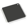
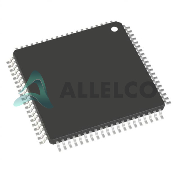
View All

Please refer to the English Version as our Official Version.Return

Europe
France(Français) Germany(Deutsch) Italy(Italia) Russian(русский) Poland(polski) Czech(Čeština) Luxembourg(Lëtzebuergesch) Netherlands(Nederland) Iceland(íslenska) Hungarian(Magyarország) Spain(español) Portugal(Português) Turkey(Türk dili) Bulgaria(Български език) Ukraine(Україна) Greece(Ελλάδα) Israel(עִבְרִית) Sweden(Svenska) Finland(Svenska) Finland(Suomi) Romania(românesc) Moldova(românesc) Slovakia(Slovenská) Denmark(Dansk) Slovenia(Slovenija) Slovenia(Hrvatska) Croatia(Hrvatska) Serbia(Hrvatska) Montenegro(Hrvatska) Bosnia and Herzegovina(Hrvatska) Lithuania(lietuvių) Spain(Português) Switzerland(Deutsch) United Kingdom(English)
Asia/Pacific
Japan(日本語) Korea(한국의) Thailand(ภาษาไทย) Malaysia(Melayu) Singapore(Melayu) Vietnam(Tiếng Việt) Philippines(Pilipino)
Africa, India and Middle East
United Arab Emirates(العربية) Iran(فارسی) Tajikistan(فارسی) India(हिंदी) Madagascar(malaɡasʲ)
South America / Oceania
New Zealand(Maori) Brazil(Português) Angola(Português) Mozambique(Português)
North America
United States(English) Canada(English) Haiti(Ayiti) Mexico(español)
HomeProductsIntegrated Circuits (ICs)Data Acquisition - Analog to Digital Converters (ADC)AD7616BSTZ
AD7616BSTZ Image
Image may be representation.
See specifications for product details.
EXPRESS OPTION
Payment method

AD7616BSTZ - Analog Devices Inc.

Manufacturer Part Number
AD7616BSTZ
Manufacturer
Analog Devices, Inc.
Allelco Part Number
32D-AD7616BSTZ
Warranty
1 Year Allelco Warranty - Find out more
Stock Status:
2,020 pcs available, New & Original
Parts Description
IC ADC 16BIT SAR 80LQFP
Package
80-LQFP (14x14)
Data sheet
AD7616BSTZ.pdf
RoHs Status
ROHS3 Compliant
Our certification
In stock: 2020
  • Unit Price: $10.40
  • Subtotal: $0.00

Want a better price?
Add to Cart and Submit RFQ now, we'll contact you immediately.

Quantity Unit Price Ext. Price
1+ $10.40 $10.40
10+ $9.09 $90.90
30+ $8.73 $261.90
90+ $8.00 $720.00
The above prices does not include taxes and freight rates, which will be calculated on the order pages.

Specifications

AD7616BSTZ Tech Specifications
Analog Devices Inc. - AD7616BSTZ technical specifications, attributes, parameters and parts with similar specifications to Analog Devices Inc. - AD7616BSTZ

Product Attribute Attribute Value
Manufacturer Analog Devices, Inc.
Voltage - Supply, Digital 2.3V ~ 3.6V
Voltage - Supply, Analog 4.75V ~ 5.25V
Supplier Device Package 80-LQFP (14x14)
Series -
Sampling Rate (Per Second) 1M
Reference Type External, Internal
Ratio - S/H:ADC -
Package / Case 80-LQFP
Package Tray
Operating Temperature -40°C ~ 125°C
Product Attribute Attribute Value
Number of Inputs 16
Number of Bits 16
Number of A/D Converters 2
Mounting Type Surface Mount
Input Type Single Ended
Features Simultaneous Sampling
Data Interface DSP, MICROWIRE™, Parallel, QSPI™, Serial, SPI™
Configuration MUX-ADC
Base Product Number AD7616
Architecture SAR

Environmental & Export Classifications

ATTRIBUTE DESCRIPTION
RoHs Status ROHS3 Compliant
Moisture Sensitivity Level (MSL) 3 (168 Hours)
REACH Status REACH Unaffected
ECCN EAR99
HTSUS 8542.39.0001

Parts Introduction

AD7616BSTZ Image
AD7616BSTZ (1)

Manufacturer Part Number

AD7616BSTZ

Manufacturer

Analog Devices

Introduction

AD7616BSTZ is a high-performance, 16-bit data acquisition system analog to digital converter (ADC) designed for high precision measurement applications.

Product Features and Performance

16-bit resolution

Sampling rate of up to 1MS/s

16 single-ended input channels

Dual ADCs allow simultaneous sampling

Supports various data interfaces including DSP, MICROWIRE™, Parallel, QSPI™, Serial, SPI™

External and Internal reference voltage options

Supports a wide range of supply voltages for analog and digital circuits

Product Advantages

High-resolution and high-speed sampling enhance measurement accuracy and system responsiveness

Simultaneous sampling capability improves system efficiency

Flexible interface options ensure compatibility with various microcontrollers and digital systems

Robust temperature range (-40°C to 125°C) ensures reliability in extreme environments

Key Technical Parameters

Number of Bits: 16

Sampling Rate (Per Second): 1M

Number of Inputs: 16

Input Type: Single Ended

Voltage - Supply, Analog: 4.75V ~ 5.25V

Voltage - Supply, Digital: 2.3V ~ 3.6V

Operating Temperature: -40°C ~ 125°C

Quality and Safety Features

Highly reliable performance across a wide temperature range ensures suitability for demanding applications

Compatibility

Compatible with DSP, MICROWIRE™, Parallel, QSPI™, Serial, and SPI™ data interfaces

Application Areas

Precision measurement systems

Data acquisition in industrial, medical, and scientific research

Embedded systems for monitoring and control

Product Lifecycle

The product status is active, indicating ongoing production and availability. Replacements or upgrades information is not specified.

Several Key Reasons to Choose This Product

High-speed and high-resolution ADC capabilities allow for precise data capture

Dual ADCs with simultaneous sampling maximize data throughput and system efficiency

Flexible interface compatibility simplifies integration with existing digital systems

Robust design ensures reliability in harsh environmental conditions

Extensive input and supply voltage ranges offer versatility for various application needs

Frequently Asked Questions(FAQ)

What are the key performance trade-offs when using the AD7616BSTZ for high-speed data acquisition in industrial environments?
The AD7616BSTZ offers a sampling rate of 1 MSPS per channel with simultaneous sampling across two SAR ADCs, making it suitable for precision applications. However, achieving this speed requires careful attention to reference stability and power supply noise, especially given its dual voltage domain design (4.75V–5.25V analog, 2.3V–3.6V digital). In industrial settings with thermal or electromagnetic interference, maintaining effective resolution demands robust decoupling and layout discipline, as even minor supply fluctuations can degrade INL and DNL beyond typical 1 LSB specifications.
How does the AD7616BSTZ compare to single-channel SAR ADCs like the AD7680 when implementing multiplexed input systems?
While the AD7616BSTZ supports 16 single-ended inputs via internal multiplexing, it differs significantly from single-channel devices such as the AD7680 in architecture and application suitability. The AD7616’s dual independent SAR converters enable true simultaneous sampling of two channels, which is critical for applications like differential measurement or phase-sensitive detection. In contrast, the AD7680 samples one input at a time, introducing timing skew in multi-channel designs. For systems requiring synchronized inputs without external switches, the AD7616BSTZ provides inherent advantages despite higher pin count and power consumption.
What layout considerations are essential when integrating the AD7616BSTZ into a mixed-signal PCB to preserve 16-bit accuracy?
Maintaining 16-bit linearity on the AD7616BSTZ necessitates strict separation between analog and digital sections on the PCB. The analog supply must be filtered with low-ESR capacitors near the package pins, and the reference input should be driven through a buffered op-amp with minimal loading to avoid settling errors. Clock traces must be short and shielded to prevent coupling into sensitive nodes, particularly since the device uses a high-speed serial interface capable of introducing jitter if poorly managed. Grounding should follow a star topology centered at the ADC, and guard rings around analog inputs help reduce leakage currents that could affect offset and gain accuracy.
Can the AD7616BSTZ operate reliably in automotive-grade temperature ranges without derating performance parameters?
Yes, the AD7616BSTZ is specified over an extended industrial temperature range of -40°C to +125°C, aligning with automotive AEC-Q100 qualification requirements. However, full performance—particularly ENOB and SFDR—depends on maintaining stable operating conditions. At elevated temperatures, input bias currents may increase slightly, potentially affecting high-impedance source compatibility unless proper buffering is implemented. Additionally, long-term reliability under thermal cycling requires adherence to Moisture Sensitivity Level 3 handling procedures during assembly to prevent popcorning damage.
What impact does reference voltage choice have on system-level error budget when using the AD7616BSTZ?
The AD7616BSTZ allows either internal or external references, but selecting an appropriate VREF directly affects achievable resolution and accuracy. An internal reference provides simplicity but typically exhibits ±0.5% initial accuracy and limited long-term drift (~30 ppm/°C), constraining overall system precision. Using an external precision reference like the LT6655 improves absolute accuracy and stability but adds cost and board space. For 16-bit effective systems, the total unadjusted error (TUE) must include quantization, INL/DNL, gain error, and reference nonlinearity; thus, a high-quality reference reduces dominant error sources and relaxes calibration needs.
How should power sequencing be managed when interfacing the AD7616BSTZ with microcontrollers supporting dynamic voltage scaling?
The AD7616BSTZ features separate analog (AVDD) and digital (DVDD) supplies with different valid ranges (4.75V–5.25V and 2.3V–3.6V respectively), necessitating careful power-up/power-down sequencing. Although the datasheet specifies no hard requirement for ordered ramp-up, best practice dictates that AVDD should reach nominal levels before or simultaneously with DVDD to prevent latch-up or input corruption due to ground bounce. During shutdown, both supplies should decay within similar timescales to avoid reverse current flow through ESD protection diodes. This is especially important in battery-powered or energy-harvesting systems where voltage rails can droop asymmetrically.
What are the implications of enabling simultaneous sampling mode in the AD7616BSTZ for signal integrity in multi-phase motor control applications?
Enabling simultaneous sampling on the AD7616BSTZ allows both ADCs to capture their respective inputs at precisely the same instant, eliminating inter-channel skew that would otherwise distort phase relationships in applications like three-phase current sensing. This is critical for accurate torque estimation and vector control algorithms. However, crosstalk between adjacent input pins—especially if routed close together—can introduce small amplitude errors or even false transitions if not properly managed through guard spacing and shielding. Proper layout and use of internal sample-and-hold circuitry minimize these effects, preserving temporal alignment across all 16 channels.
Is it feasible to daisy-chain multiple AD7616BSTZ devices using SPI-compatible interfaces for expanded channel counts?
The AD7616BSTZ supports standard SPI, QSPI, MICROWIRE, and parallel interfaces, enabling flexible communication topologies. While daisy-chaining is technically possible using the SDI/SDO pins in serial cascaded mode, practical limitations arise from propagation delay accumulation and clock stretching across devices. Each additional stage introduces timing uncertainty that may violate setup/hold margins, particularly at maximum 1 MSPS throughput. Moreover, shared CS lines complicate synchronization, and interrupt-driven conversion completion becomes harder to manage reliably. For scalable systems, dedicated chip selects per device or FPGA-based arbitration are preferred over naive daisy chaining.
How does the number of available inputs affect scalability when replacing legacy 8-channel ADCs with the AD7616BSTZ?
The AD7616BSTZ provides 16 single-ended inputs, offering double the channel density compared to many 8-channel alternatives like the AD7682. This enables consolidation of sensor arrays—such as thermocouples, strain gauges, or RTDs—onto a single IC, reducing component count and routing complexity. However, increased input capacitance (typically 4–6 pF per channel) can slow settling from high-Z sources unless buffered externally. Additionally, switching between inputs introduces aperture delay variations that may alias fast transients if not accounted for in signal chain design, particularly above 200 kSPS per channel.
What role does the internal multiplexer play in reducing external hardware when using the AD7616BSTZ?
The integrated 16-to-1 multiplexer eliminates the need for discrete analog switches or external MUX ICs, streamlining BOM and board real estate. By allowing software-controlled channel selection prior to each conversion cycle, the AD7616BSTZ simplifies firmware logic for polling multiple sensors sequentially. However, switching transients during mux transitions can induce glitches if input signals change rapidly relative to mux settling time (~100 ns typical). Careful filtering or blanking windows may be required in noisy environments to avoid corrupted conversions, adding minimal overhead to host processing.
How does the AD7616BSTZ handle common-mode voltage excursions outside its specified input range?
The AD7616BSTZ accepts input voltages from 0 V up to just below the AVDD rail, with a common-mode range defined accordingly. Exceeding these limits—either positively or negatively—can cause latch-up, permanent damage, or erratic output codes. Input protection relies on internal clamping diodes, but forward-biased conditions draw excessive current unless current-limited externally. Therefore, all input signals must remain strictly within 0 V < VIN < AVDD, even momentarily, to ensure safe operation throughout the entire operating temperature span.
What factors determine whether to choose an external versus internal reference in a precision weighing scale application using the AD7616BSTZ?
In high-precision applications like industrial scales, an external precision reference becomes necessary due to the AD7616BSTZ’s internal reference inaccuracy (±0.5%) and temperature drift. External references such as the REF5050 offer <1 ppm/°C drift and better initial accuracy (<10 ppm), directly improving load cell bridge measurement fidelity. The trade-off involves added board space and cost, but the resulting reduction in gain error and improved linearity outweighs these drawbacks when aiming for sub-milligram resolution over wide ambient conditions.
How does the AD7616BSTZ support fault detection in safety-critical monitoring systems?
Although not explicitly designed as a safety microcontroller, the AD7616BSTZ includes features useful for diagnostics: power-on reset ensures clean initialization, and its high-impedance inputs allow connection to external watchdog circuits. Host processors can implement periodic self-tests by measuring known reference voltages or injecting calibration tones. Combined with CRC-protected data frames in QSPI mode, this enables detection of conversion anomalies or communication errors—critical for functional safety certifications where deterministic behavior under fault conditions is mandated.
What are the power consumption implications of running the AD7616BSTZ continuously at full speed versus burst mode operation?
Continuous 1 MSPS operation draws approximately 15 mA from AVDD and 3 mA from DVDD under nominal conditions, totaling ~80 mW. Burst mode—where conversions occur intermittently—reduces average power significantly, beneficial in portable or low-duty-cycle applications. However, frequent wake-sleep transitions introduce startup latency (~1 µs) and transient glitches during ADC initialization, which can corrupt early samples. Designers must balance power savings against timing constraints, especially when synchronizing with other peripherals or meeting real-time deadlines.
How does the choice of interface protocol affect real-time performance when integrating the AD7616BSTZ with FPGAs?
The AD7616BSTZ supports multiple interfaces including SPI, QSPI, and parallel, each impacting data throughput and latency differently. Parallel mode offers lowest latency (~100 ns conversion plus immediate transfer), ideal for FPGA-based control loops requiring tight timing. SPI/QSPI add serialization overhead but simplify routing in dense layouts. QSPI’s quad I/O capability doubles effective bandwidth without increasing clock frequency, useful when interfacing with modern microcontrollers lacking wide GPIO banks. Choice depends on FPGA resource availability, desired throughput, and ease of timing closure.
What precautions are needed when driving the AD7616BSTZ from non-ideal signal sources like piezoelectric sensors?
Piezoelectric sensors present high output impedance and generate charge proportional to mechanical stress, making them susceptible to leakage and noise pickup. Direct connection to the AD7616BSTZ’s high-impedance inputs risks slow settling and baseline drift. Implementing a charge amplifier or FET buffer with low bias current (<1 nA) ensures adequate drive strength and preserves dynamic range. Additionally, RC filtering at the input mitigates high-frequency oscillations while maintaining response bandwidth above the signal of interest.
How does the AD7616BSTZ accommodate temperature compensation in battery management systems?
Battery voltage and internal resistance vary significantly with temperature, requiring accurate analog front ends. The AD7616BSTZ’s 16-bit resolution allows fine-grained measurement of individual cell voltages, enabling software-based lookup tables or polynomial fits to correct readings based on auxiliary temperature sensors. Its simultaneous sampling ensures consistent timestamping across multiple cells, preventing skew-induced errors in state-of-charge calculations. Coupled with low input bias current, this minimizes loading effects on high-resistance thermistor networks used for thermal modeling.
What documentation or evaluation tools are recommended for validating designs involving the AD7616BSTZ?
Analog Devices provides comprehensive evaluation boards (EVAL-AD7616EBZ) featuring breakout connectors, reference buffers, and test fixtures to characterize performance under controlled conditions. Application notes such as AN-885 detail layout guidelines and reference selection strategies, while SPICE models aid in pre-layout simulation of noise and settling behavior. Combining these resources accelerates bring-up and reduces risk of costly re-spins by identifying layout pitfalls or interface mismatches before mass production.

Parts with Similar Specifications

The three parts on the right have similar specifications to Analog Devices Inc. AD7616BSTZ

Product Attribute AD7616-PBSTZ-RL AD7616BSTZ-RL AD7616-PBSTZ AD7610BSTZ-RL
Part Number AD7616-PBSTZ-RL AD7616BSTZ-RL AD7616-PBSTZ AD7610BSTZ-RL
Manufacturer Analog Devices Inc. Analog Devices Inc. Analog Devices Inc. Analog Devices Inc.
Voltage - Supply, Analog - 3.14V ~ 3.46V 11.4V ~ 16.5V 3V ~ 3.6V
Input Type - - - Differential
Supplier Device Package - 196-NFBGA (12x12) 16-PDIP 64-VQFN (9x9)
Number of Bits - 16 8 14
Operating Temperature - -40°C ~ 85°C 0°C ~ 70°C -40°C ~ 85°C
Base Product Number - DAC34H84 MAX500 ADS62P42
Voltage - Supply, Digital - 1.14V ~ 1.26V 11.4V ~ 16.5V 1.65V ~ 3.6V
Number of A/D Converters - - - 2
Package / Case - 196-LFBGA 16-DIP (0.300', 7.62mm) 64-VFQFN Exposed Pad
Reference Type - External, Internal External External, Internal
Series - - - -
Features - - - Simultaneous Sampling
Number of Inputs - - - 2
Sampling Rate (Per Second) - - - 65M
Package - Tape & Reel (TR) Tube Tape & Reel (TR)
Ratio - S/H:ADC - - - 1:1
Data Interface - LVDS - Parallel I²C LVDS - Parallel, Parallel
Architecture - Current Source R-2R Pipelined
Configuration - - - S/H-ADC
Mounting Type - Surface Mount Through Hole Surface Mount

AD7616BSTZ Datasheet PDF

Download AD7616BSTZ pdf datasheets and Analog Devices Inc. documentation for AD7616BSTZ - Analog Devices Inc..

Datasheets
AD7616.pdf
PCN Assembly/Origin
LQFP_EP/MQFP 08/Dec/2016.pdf
Other Related Documents
Manipulating MCU SPI Interface to Access a Nonstan.pdf

Customer Reviews

Evaluation: 10 Articles

  • Nath***rooks
    Jun 11, 2026

    Installed this power component in a converter board. Output remained stable under different load conditions and thermal performance was better than expected.

  • Dani***alkerTech
    Jun 1, 2026

    Product works, but setup took more effort than expected. Once configured the MCU ran reliably, although documentation support felt older compared with newer platforms. Fine for maintenance projects.

  • Yuki***aka88
    May 26, 2026

    信号通信プロジェクトでこのRS-485トランシーバーを使用しました。設置は簡単で、長距離ケーブルでも通信は安定していました。消費電力も、以前使用していたものより低くなっています。

  • Stev***aker
    May 20, 2026

    Solid diode for power rectification. Works well in switching circuits.

  • Bran***Lewis
    May 11, 2026

    Compact FPGA with good performance. Suitable for basic signal processing tasks.

  • Oliv***arris
    May 7, 2026

    Reliable I/O expander. Works well in embedded control applications.

  • Jess***Jones
    Apr 17, 2026

    It offers good value for the price, and the specifications match the description. I’ve been using it for two days with no issues, and I’ll definitely buy it again if I need it in the future.

  • Mich***Smith
    Apr 17, 2026

    Shipping was on time, the component pins are neatly aligned, and I tested 10 of them with a multimeter—all readings were within the specified range. Highly recommended.

  • Aman***arris
    Apr 3, 2026

    It was great—the entire process, from placing the order to receiving the package, went very smoothly. The components were consistent, the price was fair, and I had a very pleasant shopping experience.

  • Mike***nch
    Apr 3, 2026

    Better than expected! The resistance and capacitance readings were spot-on, and it passed the test on the first try. The service was reliable, and the packaging was thoughtful—I highly recommend it.

Write a Review

Your Email address will not be published.

Shipment

Delivery Time

In-stock items can be shipped within 24 hours. Some parts will be arranged for delivery within 1-2 days from the date all items arrive at our warehouse. And Allelco ships order once a day at about 17:00, except Sunday. Once the goods are shipped, the estimated delivery time depends on the shipping methods and Delivery destination. The table below shows are the logistic time for some common countries.

Delivery Cost

  1. Use your express account for shipment if you have one.
  2. Use our account for the shipment. Refer to the table below for the approximate charges.
(Different time frame / countries / package size has different price.)

Delivery Method

  1. Global Common Shipment by DHL / UPS / FedEx / TNT / EMS / SF we support.
  2. Others more shipping ways, please get in touch with your customer manager.

Common Countries Logistic Time Reference
Region Country Logistic Time(Day)
America United States 5
Brazil 7
Europe Germany 5
United Kingdom 4
Italy 5
Oceania Australia 6
New Zealand 5
Asia India 4
Japan 4
Middle East Israel 6
DHL & FedEx Shipment Charges Reference
Shipment charges(KG) Reference DHL(USD$)
0.00kg-1.00kg USD$30.00 - USD$60.00
1.00kg-2.00kg USD$40.00 - USD$80.00
2.00kg-3.00kg USD$50.00 - USD$100.00
Note:
The above table is for reference only. There may have some data bias for the uncontrollable factors.
Contact us if you have any questions.
  • QC (Quality Warranty)
  • Payment Support
  • Packaging
  • Certifications & Memberships

QC (Quality Warranty)

Allelco is committed to exceeding customer expectations through customer service excellence, order accuracy, and on-time delivery.
This is achieved through our commitment to the continual improvement of our processes, services, and products.


Strict quality inspection builds a solid foundation for electronic component quality.
  1. Visual inspection
  2. Performance testing and reliability verification
  3. Standardized full-process testing
  4. Precise control of every parameter
We eliminate defective components and ensure the stable operation of electronic devices through professional quality standards.

Payment Support

The payment method can be chosen from the methods shown below: Wire Transfer (T/T, Bank Transfer), Western Union, Credit card, PayPal.
  • HKBea
  • Paypal
  • MasterCard
  • Western-Union
  • VISA
Stable Delivery, Sincere Partnership — Your Faithful Supply Chain Partner
  • Efficient Supply Management
  • Cost-Saving Procurement
  • Fast Sourcing & Delivery
Contact us if you have any questions.

Packaging

Electrostatic Discharge Protection and Handling

All electrostatic-sensitive components are handled in accordance with electrostatic discharge control procedures. The products are hermetically sealed in anti-static safe packaging to prevent electrostatic damage. Appropriate labeling is also applied for identification and traceability. This ensures product integrity during storage, handling and transportation.


ESD

Certifications & Memberships

Third-party certified, strict quality control. Our certification
  • ISO 9001: 2015
  • ISO 13485: 2016
  • ISO 14001: 2015
  • ISO 28000: 2007
  • ISO 45001: 2018
  • GB/T 27922-2011
  • SMTA
  • IPC
  • ESD
  • PSMA
AD7616BSTZ Image

AD7616BSTZ

Analog Devices Inc.
32D-AD7616BSTZ

Want a better price? Add to Cart and Submit RFQ now, we'll contact you immediately.

0 RFQ
Shopping cart (0 Items)
It is empty.
Compare List (0 Items)
It is empty.
Feedback

Your feedback matters! At Allelco, we value the user experience and strive to improve it constantly.
Please share your comments with us via our feedback form, and we'll respond promptly.
Thank you for choosing Allelco.

Subject
E-mail
Comments
Captcha
Drag or click to upload file
Upload File
types: .xls, .xlsx, .doc, .docx, .jpg, .png and .pdf.
Max file size: 10MB