

 AD8610ARZ-REEL7Analog Devices Inc.IC OPAMP JFET 1 CIRCUIT 8SOIC
 AD8609ARUZ-REELAnalog Devices Inc.IC CMOS 4 CIRCUIT 14TSSOP
 AD8609ARZ-REEL7Analog Devices Inc.IC CMOS 4 CIRCUIT 14SOIC
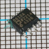 AD8610ARZAnalog Devices Inc.IC OPAMP JFET 1 CIRCUIT 8SOIC
 AD8609ARZAnalog Devices Inc.IC CMOS 4 CIRCUIT 14SOIC
- Dani***alkerTech
- Jun 1, 2026
HomeProductsIntegrated Circuits (ICs)Linear - Amplifiers - Instrumentation, OP Amps, Buffer AmpsAD8610ARM-R2


Image may be representation.
See specifications for product details.
See specifications for product details.
- EXPRESS OPTION
- Payment method
AD8610ARM-R2 - Analog Devices Inc.
- Manufacturer Part Number
- AD8610ARM-R2
- Manufacturer
- Analog Devices, Inc.
- Allelco Part Number
- 98D-AD8610ARM-R2
- Warranty
- 1 Year Allelco Warranty - Find out more
- Stock Status:
- 38,598 pcs available, New & Original
- Parts Description
- IC OPAMP JFET 25MHZ PREC 8MSOP
- Package
- 8-MSOP
- Data sheet
-
AD8610ARM-R2.pdf
Datasheets
AD8610, 20 Datasheet.pdfOther Related Documents
Tape and Reel Packaging.pdfDesign Resources
Precision, AC Reference Signal Attenuator Using AD.pdf
- RoHs Status
- Our certification
- In stock: 38598
- Unit Price: $4.77
- Subtotal: $0.00
Want a better price?
Add to Cart and Submit RFQ now, we'll contact you immediately.
| Quantity | Unit Price | Ext. Price |
|---|---|---|
| 1+ | $4.77 | $4.77 |
| 250+ | $1.846 | $461.50 |
| 500+ | $1.781 | $890.50 |
| 1000+ | $1.749 | $1,749.00 |
The above prices does not include taxes and freight rates, which will be calculated on the order pages.


