View All

Please refer to the English Version as our Official Version.Return

Europe
France(Français) Germany(Deutsch) Italy(Italia) Russian(русский) Poland(polski) Czech(Čeština) Luxembourg(Lëtzebuergesch) Netherlands(Nederland) Iceland(íslenska) Hungarian(Magyarország) Spain(español) Portugal(Português) Turkey(Türk dili) Bulgaria(Български език) Ukraine(Україна) Greece(Ελλάδα) Israel(עִבְרִית) Sweden(Svenska) Finland(Svenska) Finland(Suomi) Romania(românesc) Moldova(românesc) Slovakia(Slovenská) Denmark(Dansk) Slovenia(Slovenija) Slovenia(Hrvatska) Croatia(Hrvatska) Serbia(Hrvatska) Montenegro(Hrvatska) Bosnia and Herzegovina(Hrvatska) Lithuania(lietuvių) Spain(Português) Switzerland(Deutsch) United Kingdom(English)
Asia/Pacific
Japan(日本語) Korea(한국의) Thailand(ภาษาไทย) Malaysia(Melayu) Singapore(Melayu) Vietnam(Tiếng Việt) Philippines(Pilipino)
Africa, India and Middle East
United Arab Emirates(العربية) Iran(فارسی) Tajikistan(فارسی) India(हिंदी) Madagascar(malaɡasʲ)
South America / Oceania
New Zealand(Maori) Brazil(Português) Angola(Português) Mozambique(Português)
North America
United States(English) Canada(English) Haiti(Ayiti) Mexico(español)
HomeProductsIntegrated Circuits (ICs)Data Acquisition - Analog to Digital Converters (ADC)AD9228BCPZ-40
AD9228BCPZ-40 Image
Image may be representation.
See specifications for product details.
EXPRESS OPTION
Payment method

AD9228BCPZ-40 - Analog Devices Inc.

Manufacturer Part Number
AD9228BCPZ-40
Manufacturer
Analog Devices, Inc.
Allelco Part Number
32D-AD9228BCPZ-40
Warranty
1 Year Allelco Warranty - Find out more
Stock Status:
5,560 pcs available, New & Original
Parts Description
IC ADC LVDS 12BIT QUAD 48LFCSP
Package
48-LFCSP-VQ (7x7)
Data sheet
AD9228BCPZ-40.pdf

Datasheets

AD9228.pdf

HTML Datasheet

AD9228.pdf

PCN Obsolescence/ EOL

Multiple Families 12/Mar/2010.pdf
RoHs Status
 
Our certification
In stock: 5560

Required fields are indicated by an asterisk (*)
Please send RFQ, we will respond immediately.

Quantity

Specifications

AD9228BCPZ-40 Tech Specifications
Analog Devices Inc. - AD9228BCPZ-40 technical specifications, attributes, parameters and parts with similar specifications to Analog Devices Inc. - AD9228BCPZ-40

Product Attribute Attribute Value
Manufacturer Analog Devices, Inc.
Supplier Device Package 48-LFCSP-VQ (7x7)
Series -
Sampling Rate (Per Second) 40M
Package / Case 48-VFQFN Exposed Pad, CSP
Package Tray
Product Attribute Attribute Value
Operating Temperature -40°C ~ 85°C
Number of Bits 12
Number of A/D Converters 4
Mounting Type Surface Mount
Data Interface SPI
Base Product Number AD9228

Environmental & Export Classifications

ATTRIBUTE DESCRIPTION
Moisture Sensitivity Level (MSL) 6 (Time on Label)
ECCN EAR99
HTSUS 8542.39.0001

Parts Introduction

AD9228BCPZ-40 Image
AD9228BCPZ-40 (1)

Manufacturer Part Number

AD9228BCPZ-40

Manufacturer

Analog Devices, Inc.

Introduction

The AD9228 is a high-performance, 12-bit, 4-channel, 40 MSPS analog-to-digital converter (ADC) designed for applications requiring high speed, high dynamic range, and low power consumption.

Product Features and Performance

12-bit resolution

40 MSPS sampling rate

4 independent input channels

Low power consumption

High dynamic range

Wide operating temperature range (-40°C to 85°C)

Product Advantages

Excellent signal-to-noise ratio (SNR) and spurious-free dynamic range (SFDR)

Integrated low-noise, high-bandwidth input buffer amplifiers

Flexible digital interface (SPI)

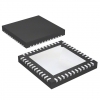
Small package size (48-LFCSP-VQ)

Key Technical Parameters

Resolution: 12 bits

Sampling Rate: 40 MSPS

Number of Channels: 4

Data Interface: SPI

Package: 48-LFCSP-VQ (7x7)

Operating Temperature: -40°C to 85°C

Quality and Safety Features

Robust design for reliable operation

Compliance with industry standards

Thorough testing and quality control measures

Compatibility

The AD9228 is compatible with a wide range of digital signal processing (DSP) and microcontroller-based systems.

Application Areas

Medical imaging equipment

Industrial automation and control systems

Test and measurement equipment

Communications systems

Instrumentation and data acquisition

Product Lifecycle

The AD9228 is an active product and is not nearing discontinuation. Replacement or upgraded models may be available in the future.

Key Reasons to Choose This Product

High-performance 12-bit, 4-channel ADC with excellent signal quality

Low power consumption and compact package size

Wide operating temperature range for diverse applications

Flexible digital interface and compatibility with various systems

Reliable and well-tested design for consistent performance
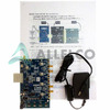
Frequently Asked Questions(FAQ)

How does the AD9228BCPZ-40 handle input signal integrity at its maximum sampling rate of 40MHz, and what design considerations are needed to maintain effective conversion accuracy?
At 40MSPS, the AD9228BCPZ-40 requires careful attention to analog front-end layout and impedance matching due to its 12-bit resolution and 0.4LSB integral nonlinearity specification. The device operates from a single 1.7V to 1.9V supply, which necessitates precision biasing and noise filtering at the input stage. PCB trace length matching and controlled source impedance are critical to prevent aperture jitter and ensure that differential signals remain within the expected dynamic range. Without proper termination and shielding, high-frequency noise can degrade effective number of bits (ENOB), particularly in bandwidth-limited applications such as sensor signal acquisition or communications systems.
In comparison to higher-speed 12-bit ADCs, how does the AD9228BCPZ-40 balance power consumption, noise performance, and sampling rate for mid-bandwidth embedded systems?
Compared to devices like the AD9238 (65MSPS) or AD9257 (125MSPS), the AD9228BCPZ-40 trades peak throughput for lower power and reduced complexity, making it suitable for applications where 40MSPS is sufficient—such as industrial motor control or battery-powered instrumentation. While faster converters often use dual-supply architectures and higher current budgets to achieve lower distortion at elevated rates, the AD9228BCPZ-40 achieves its performance within a tightly constrained 1.7–1.9V rail, minimizing voltage headroom loss. This results in a favorable power-delay product for moderate-speed designs but may not scale efficiently into wideband RF sampling scenarios.
What impact does temperature variation across the -40°C to +85°C operating range have on the AD9228BCPZ-40's linearity and offset stability, and how should this be compensated in system calibration?
Over the full industrial temperature span, the AD9228BCPZ-40 exhibits predictable drift in DC offset and gain characteristics, consistent with typical bipolar junction transistor-based internal reference structures. Users should expect offset shifts on the order of tens of millivolts without trimming, while gain errors may accumulate beyond 1 LSB in extreme corners. System-level calibration using background or foreground techniques—such as injecting known DC levels or leveraging internal diagnostic modes—is recommended to preserve measurement accuracy. Temperature sensors paired with lookup tables can dynamically adjust correction coefficients based on real-time conditions.
Can the AD9228BCPZ-40 support true differential inputs, and if so, how does this configuration improve noise immunity compared to single-ended operation in noisy industrial environments?
Yes, the AD9228BCPZ-40 supports fully differential input architecture when driven appropriately through matched resistors or transformer-coupled sources. Differential signaling rejects common-mode noise and ground bounce by canceling out even-order harmonics and electromagnetic interference present on both signal lines. When implemented correctly with balanced impedances and symmetric routing, this topology improves spurious-free dynamic range (SFDR) by several decibels, especially above 10MHz. However, the benefit diminishes if the analog input driver lacks common-mode rejection or if layout symmetry is compromised.
How many clock cycles are required for the AD9228BCPZ-40 to stabilize after power-up, and what precautions should be taken during startup sequencing to avoid data corruption?
The AD9228BCPZ-40 typically requires approximately 10,000 to 50,000 clock cycles for internal bias circuits and reference settling, depending on external load capacitance and power supply ramp characteristics. To prevent transient output codes or invalid data during initialization, designers should apply a minimum hold-off period after asserting the clock before capturing first valid samples. Additionally, ensuring that the core voltage (AVDD) reaches within ±5% of nominal before enabling digital outputs reduces the risk of latch-up or metastability in downstream logic interfaces.
What is the maximum allowable input voltage swing for the AD9228BCPZ-40, and how does exceeding this limit affect ADC performance and long-term reliability?
The absolute maximum differential input voltage is ±1.0Vpp centered around the analog ground (AGND). Exceeding this range causes clipping at the input stages, leading to harmonic distortion, reduced SFDR, and increased total harmonic distortion (THD). Prolonged overdrive may also stress ESD protection diodes, potentially degrading input circuitry over time. For best results, the input signal should be scaled to utilize the full 12-bit dynamic range without approaching saturation, typically achieved by setting a 1.0Vpp full-scale sine wave amplitude at the ADC input pins.
How does the AD9228BCPZ-40 interface with standard serial digital output protocols, and what configuration options exist for adjusting data alignment and timing?
The AD9228BCPZ-40 provides flexible serial output via LVDS-compatible CMOS or low-voltage differential signaling (LVDS) depending on package pin assignments and mode selection through SPI register settings. Data can be aligned to rising or falling clock edges, and output delay can be fine-tuned using programmable deserializer timing controls. This flexibility allows synchronization with FPGA or ASIC capture blocks operating at various phase relationships, though care must be taken to maintain setup and hold margins relative to the 40MHz clock edge rate.
What is the typical power dissipation of the AD9228BCPZ-40 when operating at 40MSPS with all channels active, and how does this compare to similar ADCs in terms of efficiency?
At 40MSPS with all four channels enabled and default internal termination, the AD9228BCPZ-40 consumes approximately 35mW from the 1.8V supply. This equates to about 0.88mW per MSPS per channel, placing it among the more power-efficient 12-bit ADCs in its class. Devices such as the ADS54J60 consume significantly more power (~120mW at 65MSPS) due to higher linearity requirements and dual-supply architectures, making the AD9228BCPZ-40 advantageous for energy-constrained portable or battery-operated measurement systems.
Are there any known limitations in using the AD9228BCPZ-40 for direct RF sampling applications above 10MHz, and what modifications would be necessary to enable such use?
Direct RF sampling above 10MHz is feasible only with significant front-end conditioning. The AD9228BCPZ-40 lacks built-in anti-alias filters and has limited Nyquist zone rejection, so broadband RF signals require careful analog pre-filtering and possibly downconversion before reaching the ADC inputs. Additionally, clock jitter becomes critical above 10MHz; the internal PLL must be bypassed in favor of an ultra-low-jitter external clock source to maintain SFDR. Without these enhancements, imaging and aliasing artifacts will dominate the output spectrum.
How should decoupling capacitors be selected and placed for optimal performance of the AD9228BCPZ-40, considering its LFCSP-48-VQ(7x7) package and mixed-signal nature?
Due to the small 7mm × 7mm footprint and high pin density of the LFCSP package, high-frequency decoupling is essential near each power pin. A combination of 0.1µF ceramic capacitors rated for 4V or higher, along with 1nF to 10nF MLCCs for broadband suppression, should be placed directly adjacent to AVDD and DVDD pins. These must be connected to separate analog and digital ground planes joined at a single point near the ADC to minimize ground loop inductance. Avoid long traces and vias in the return path to maintain low impedance at frequencies up to 1GHz.
Can multiple AD9228BCPZ-40 devices be synchronized for multi-channel data acquisition, and what features support coherent sampling across units?
Limited synchronization is possible through shared clock and trigger signals, but the AD9228BCPZ-40 does not include advanced features like daisy-chaining or integrated sample-and-hold delays across channels or devices. Coherent operation requires external master timing control with precise alignment of clock edges and strobe pulses. Variations in internal propagation delay between channels (typically <20ps) are usually acceptable for sub-microsecond timing accuracy, but applications requiring picosecond-level correlation may need alternative architectures or dedicated synchronization ICs.
What role does the internal reference play in the AD9228BCPZ-40, and under what conditions might external reference usage improve system accuracy?
The AD9228BCPZ-40 includes a bandgap-based internal reference offering adequate stability (±25ppm/°C typical) for general-purpose applications. However, in precision measurement systems requiring better than ±10ppm/°C long-term stability or tighter gain tracking across temperature, an external precision reference such as the ADR4550 should be employed. External references eliminate ADC-to-ADC variation and provide tighter initial tolerance, improving overall system linearity and reducing calibration overhead in multi-unit deployments.
How does the AD9228BCPZ-40 handle digital output transitions during power-down versus normal operation, and what precautions prevent bus contention in shared digital busses?
During normal operation, digital outputs transition cleanly with minimal ringing due to integrated slew-rate control. In power-down mode, outputs enter high-impedance state rapidly, preventing back-driving of other devices. However, simultaneous switching of multiple ADCs sharing a common bus can induce crosstalk unless series termination resistors (e.g., 22Ω) are used near each output. Additionally, enabling output drivers only when downstream receivers are ready minimizes glitching during enable transitions.
What is the minimum hold time required for the input signal before a conversion begins on the AD9228BCPZ-40, and how is this related to aperture uncertainty?
The AD9228BCPZ-40 has an aperture uncertainty of approximately 15ps RMS, corresponding to a minimum effective signal stabilization window of ~3–5ns for reliable conversion. While the datasheet does not specify a formal "hold time," the input sampling instant occurs just before the rising edge of the clock, so the analog signal must settle within this narrow window. This implies that the source impedance should be low enough to allow settling within 0.5 LSB error, typically requiring RC time constants below 100ps for high-precision applications.
How do layout parasitics in the PCB affect the performance of the AD9228BCPZ-40, particularly regarding input impedance and clock distribution?
Parasitic inductance and capacitance in the analog input network can resonate with termination resistors, creating peaking or attenuation peaks near the Nyquist frequency (20MHz). Similarly, clock trace inductance can increase jitter when driving the ADC’s input buffer. Both effects degrade SFDR and ENOB. Best practices include keeping input traces short (<10mm), avoiding vias in signal paths, using guard rings around sensitive nets, and routing clock lines with matched lengths and controlled impedance (typically 50Ω single-ended).
Is the AD9228BCPZ-40 suitable for medical imaging or ultrasound systems, and what additional components would be required to meet those application demands?
While technically capable of processing signals relevant to ultrasonic echo detection, the AD9228BCPZ-40 alone is insufficient for medical imaging without substantial augmentation. It lacks ultra-low-noise front-end drivers, programmable gain amplifiers (PGAs), and integrated anti-aliasing filters. Furthermore, medical standards impose strict safety and EMI requirements that demand isolated power supplies and reinforced creepage distances. Therefore, a complete subsystem including driver ICs, baluns, and FPGA-based beamforming would be needed alongside the AD9228BCPZ-40 to meet clinical certification criteria.

Parts with Similar Specifications

The three parts on the right have similar specifications to Analog Devices Inc. AD9228BCPZ-40

Product Attribute AD9228ABCPZ-40 AD9228BCPZRL7-40 AD9228ABCPZRL7-40 AD9229BCPZ-50
Part Number AD9228ABCPZ-40 AD9228BCPZRL7-40 AD9228ABCPZRL7-40 AD9229BCPZ-50
Manufacturer Analog Devices Inc. Analog Devices Inc. Analog Devices Inc. Analog Devices Inc.
Series - - - -
Package - Tape & Reel (TR) Tube Tape & Reel (TR)
Package / Case - 196-LFBGA 16-DIP (0.300', 7.62mm) 64-VFQFN Exposed Pad
Mounting Type - Surface Mount Through Hole Surface Mount
Number of Bits - 16 8 14
Supplier Device Package - 196-NFBGA (12x12) 16-PDIP 64-VQFN (9x9)
Sampling Rate (Per Second) - - - 65M
Number of A/D Converters - - - 2
Operating Temperature - -40°C ~ 85°C 0°C ~ 70°C -40°C ~ 85°C
Base Product Number - DAC34H84 MAX500 ADS62P42
Data Interface - LVDS - Parallel I²C LVDS - Parallel, Parallel

AD9228BCPZ-40 Datasheet PDF

Download AD9228BCPZ-40 pdf datasheets and Analog Devices Inc. documentation for AD9228BCPZ-40 - Analog Devices Inc..

Datasheets
AD9228.pdf
HTML Datasheet
AD9228.pdf
PCN Obsolescence/ EOL
Multiple Families 12/Mar/2010.pdf

Customer Reviews

Evaluation: 10 Articles

  • Emil***rperTech
    Jun 23, 2026

    Works exactly as described. I used it as a USB-to-SPI bridge in a small MCU development project and communication was stable from the first setup.

  • Liam***terTech
    Jun 15, 2026

    Used this CPLD in a logic control project. Programming was straightforward and signal timing matched the design requirements.

  • Nath***rooks
    Jun 11, 2026

    Installed this power component in a converter board. Output remained stable under different load conditions and thermal performance was better than expected.

  • Dani***alkerTech
    Jun 1, 2026

    Product works, but setup took more effort than expected. Once configured the MCU ran reliably, although documentation support felt older compared with newer platforms. Fine for maintenance projects.

  • Yuki***aka88
    May 26, 2026

    信号通信プロジェクトでこのRS-485トランシーバーを使用しました。設置は簡単で、長距離ケーブルでも通信は安定していました。消費電力も、以前使用していたものより低くなっています。

  • Stev***aker
    May 20, 2026

    Solid diode for power rectification. Works well in switching circuits.

  • Bran***Lewis
    May 11, 2026

    Compact FPGA with good performance. Suitable for basic signal processing tasks.

  • Oliv***arris
    May 7, 2026

    Reliable I/O expander. Works well in embedded control applications.

  • Jess***Jones
    Apr 17, 2026

    It offers good value for the price, and the specifications match the description. I’ve been using it for two days with no issues, and I’ll definitely buy it again if I need it in the future.

  • Mich***Smith
    Apr 17, 2026

    Shipping was on time, the component pins are neatly aligned, and I tested 10 of them with a multimeter—all readings were within the specified range. Highly recommended.

Write a Review

Your Email address will not be published.

Shipment

Delivery Time

In-stock items can be shipped within 24 hours. Some parts will be arranged for delivery within 1-2 days from the date all items arrive at our warehouse. And Allelco ships order once a day at about 17:00, except Sunday. Once the goods are shipped, the estimated delivery time depends on the shipping methods and Delivery destination. The table below shows are the logistic time for some common countries.

Delivery Cost

  1. Use your express account for shipment if you have one.
  2. Use our account for the shipment. Refer to the table below for the approximate charges.
(Different time frame / countries / package size has different price.)

Delivery Method

  1. Global Common Shipment by DHL / UPS / FedEx / TNT / EMS / SF we support.
  2. Others more shipping ways, please get in touch with your customer manager.

Common Countries Logistic Time Reference
Region Country Logistic Time(Day)
America United States 5
Brazil 7
Europe Germany 5
United Kingdom 4
Italy 5
Oceania Australia 6
New Zealand 5
Asia India 4
Japan 4
Middle East Israel 6
DHL & FedEx Shipment Charges Reference
Shipment charges(KG) Reference DHL(USD$)
0.00kg-1.00kg USD$30.00 - USD$60.00
1.00kg-2.00kg USD$40.00 - USD$80.00
2.00kg-3.00kg USD$50.00 - USD$100.00
Note:
The above table is for reference only. There may have some data bias for the uncontrollable factors.
Contact us if you have any questions.
  • QC (Quality Warranty)
  • Payment Support
  • Packaging
  • Certifications & Memberships

QC (Quality Warranty)

Allelco is committed to exceeding customer expectations through customer service excellence, order accuracy, and on-time delivery.
This is achieved through our commitment to the continual improvement of our processes, services, and products.


Strict quality inspection builds a solid foundation for electronic component quality.
  1. Visual inspection
  2. Performance testing and reliability verification
  3. Standardized full-process testing
  4. Precise control of every parameter
We eliminate defective components and ensure the stable operation of electronic devices through professional quality standards.

Payment Support

The payment method can be chosen from the methods shown below: Wire Transfer (T/T, Bank Transfer), Western Union, Credit card, PayPal.
  • HKBea
  • Paypal
  • MasterCard
  • Western-Union
  • VISA
Stable Delivery, Sincere Partnership — Your Faithful Supply Chain Partner
  • Efficient Supply Management
  • Cost-Saving Procurement
  • Fast Sourcing & Delivery
Contact us if you have any questions.

Packaging

Electrostatic Discharge Protection and Handling

All electrostatic-sensitive components are handled in accordance with electrostatic discharge control procedures. The products are hermetically sealed in anti-static safe packaging to prevent electrostatic damage. Appropriate labeling is also applied for identification and traceability. This ensures product integrity during storage, handling and transportation.


ESD

Certifications & Memberships

Third-party certified, strict quality control. Our certification
  • ISO 9001: 2015
  • ISO 13485: 2016
  • ISO 14001: 2015
  • ISO 28000: 2007
  • ISO 45001: 2018
  • GB/T 27922-2011
  • SMTA
  • IPC
  • ESD
  • PSMA
AD9228BCPZ-40 Image

AD9228BCPZ-40

Analog Devices Inc.
32D-AD9228BCPZ-40

Want a better price? Add to Cart and Submit RFQ now, we'll contact you immediately.

0 RFQ
Shopping cart (0 Items)
It is empty.
Compare List (0 Items)
It is empty.
Feedback

Your feedback matters! At Allelco, we value the user experience and strive to improve it constantly.
Please share your comments with us via our feedback form, and we'll respond promptly.
Thank you for choosing Allelco.

Subject
E-mail
Comments
Captcha
Drag or click to upload file
Upload File
types: .xls, .xlsx, .doc, .docx, .jpg, .png and .pdf.
Max file size: 10MB