View All

Please refer to the English Version as our Official Version.Return

Europe
France(Français) Germany(Deutsch) Italy(Italia) Russian(русский) Poland(polski) Czech(Čeština) Luxembourg(Lëtzebuergesch) Netherlands(Nederland) Iceland(íslenska) Hungarian(Magyarország) Spain(español) Portugal(Português) Turkey(Türk dili) Bulgaria(Български език) Ukraine(Україна) Greece(Ελλάδα) Israel(עִבְרִית) Sweden(Svenska) Finland(Svenska) Finland(Suomi) Romania(românesc) Moldova(românesc) Slovakia(Slovenská) Denmark(Dansk) Slovenia(Slovenija) Slovenia(Hrvatska) Croatia(Hrvatska) Serbia(Hrvatska) Montenegro(Hrvatska) Bosnia and Herzegovina(Hrvatska) Lithuania(lietuvių) Spain(Português) Switzerland(Deutsch) United Kingdom(English)
Asia/Pacific
Japan(日本語) Korea(한국의) Thailand(ภาษาไทย) Malaysia(Melayu) Singapore(Melayu) Vietnam(Tiếng Việt) Philippines(Pilipino)
Africa, India and Middle East
United Arab Emirates(العربية) Iran(فارسی) Tajikistan(فارسی) India(हिंदी) Madagascar(malaɡasʲ)
South America / Oceania
New Zealand(Maori) Brazil(Português) Angola(Português) Mozambique(Português)
North America
United States(English) Canada(English) Haiti(Ayiti) Mexico(español)
HomeProductsRF/IF and RFIDRF AmplifiersADL8111ACCZN
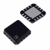
ADL8111ACCZN Image
Image may be representation.
See specifications for product details.
EXPRESS OPTION
Payment method

ADL8111ACCZN - Analog Devices Inc.

Manufacturer Part Number
ADL8111ACCZN
Manufacturer
Analog Devices, Inc.
Allelco Part Number
32D-ADL8111ACCZN
Warranty
1 Year Allelco Warranty - Find out more
Stock Status:
28,159 pcs available, New & Original
Parts Description
IC RF AMP GPS 10MHZ-8GHZ 28LGA
Package
28-LGA (6x6)
Data sheet
ADL8111ACCZN.pdf
RoHs Status
ROHS3 Compliant
Our certification
In stock: 28159
  • Unit Price: $63.49
  • Subtotal: $0.00

Want a better price?
Add to Cart and Submit RFQ now, we'll contact you immediately.

Quantity Unit Price Ext. Price
1+ $63.49 $63.49
100+ $63.49 $6,349.00
The above prices does not include taxes and freight rates, which will be calculated on the order pages.

Specifications

ADL8111ACCZN Tech Specifications
Analog Devices Inc. - ADL8111ACCZN technical specifications, attributes, parameters and parts with similar specifications to Analog Devices Inc. - ADL8111ACCZN

Product Attribute Attribute Value
Manufacturer Analog Devices, Inc.
Voltage - Supply 3V ~ 5.5V
Test Frequency 10MHz ~ 5GHz
Supplier Device Package 28-LGA (6x6)
Series -
RF Type General Purpose
Package / Case 28-LFLGA Exposed Pad
Package Strip
Product Attribute Attribute Value
P1dB 19.5dBm
Noise Figure 4.5dB
Mounting Type Surface Mount
Gain 11.5dB
Frequency 10MHz ~ 8GHz
Current - Supply 70mA
Base Product Number ADL8111

Environmental & Export Classifications

ATTRIBUTE DESCRIPTION
RoHs Status ROHS3 Compliant
Moisture Sensitivity Level (MSL) 3 (168 Hours)
REACH Status REACH Unaffected
ECCN EAR99
HTSUS 8542.33.0001

Parts Introduction

ADL8111ACCZN Image
ADL8111ACCZN (1)

Manufacturer Part Number

ADL8111ACCZN

Manufacturer

Analog Devices, Inc.

Introduction

High-performance, wideband RF amplifier covering 10 MHz to 8 GHz frequency range

Product Features and Performance

Gain of 11.5 dB

Noise figure of 4.5 dB

P1dB of 19.5 dBm

Supports 3 V to 5.5 V supply voltage

Typical current consumption of 70 mA

Product Advantages

Broad frequency coverage from 10 MHz to 8 GHz

High gain and low noise figure

Suitable for general-purpose RF applications

Key Technical Parameters

Frequency range: 10 MHz to 8 GHz

Gain: 11.5 dB

Noise figure: 4.5 dB

P1dB: 19.5 dBm

Supply voltage: 3 V to 5.5 V

Supply current: 70 mA

Quality and Safety Features

RoHS3 compliant

28-LGA (6x6) package

Compatibility

Suitable for surface mount applications

Application Areas

Suitable for a wide range of RF applications, including wireless communication systems, test and measurement equipment, and other general-purpose RF circuits

Product Lifecycle

This product is currently available and not nearing discontinuation.

Key Reasons to Choose This Product

Broad frequency coverage from 10 MHz to 8 GHz

High gain and low noise figure

Suitable for general-purpose RF applications

RoHS3 compliant

Available in a compact 28-LGA (6x6) package

Frequently Asked Questions(FAQ)

What are the key performance trade-offs when selecting the ADL8111ACCZN for a GPS receiver front-end operating at 1.575 GHz?
The ADL8111ACCZN offers a gain of 11.5 dB and a noise figure of 4.5 dB, which are favorable for low-noise amplification in GPS applications. However, its output power at 1 dB compression (P1dB) is 19.5 dBm, indicating limited linearity under high input levels. In a GPS system with weak signal reception (~-160 dBm), this device can preserve signal integrity due to low noise, but designers must ensure input levels remain below -8 dBm to avoid compression, especially in environments with strong interfering signals. The supply current of 70 mA at 3V adds to power consumption, which may require thermal or battery life considerations in portable devices.
How does the ADL8111ACCZN compare to the ADL8110 in terms of noise figure and dynamic range for use in a wideband RF front-end from 10 MHz to 5 GHz?
While both the ADL8111ACCZN and ADL8110 are part of the same product family, the ADL8111 typically achieves a slightly lower noise figure (4.5 dB vs. ~5.0 dB) and comparable P1dB (19.5 dBm vs. 19.0 dBm), making it better suited for applications demanding higher sensitivity. The ADL8111 also supports a broader frequency range (up to 8 GHz), whereas the ADL8110 is generally rated to 5 GHz. For a wideband front-end covering 10 MHz to 5 GHz, the ADL8111ACCZN provides superior linearity and noise performance, reducing the need for additional pre-amplification stages, thus simplifying the design.
What layout considerations are critical when integrating the ADL8111ACCZN in a 28-LGA (6x6) package to maintain RF performance?
The ADL8111ACCZN's exposed pad requires careful PCB grounding to minimize inductance and ensure effective heat dissipation. A solid ground plane beneath the 28-LGA package reduces ground loop inductance and improves RF stability. Impedance matching networks at the input and output should be placed as close as possible to the pins to minimize trace length and parasitic effects. Given the wide bandwidth (10 MHz to 8 GHz), even minor discontinuities can cause reflections; therefore, controlled-impedance routing and minimal via usage near RF traces are essential to preserve gain and return loss.
Can the ADL8111ACCZN be used in a multi-stage amplifier chain for a satellite communication system requiring cumulative gain above 25 dB?
Yes, the ADL8111ACCZN can serve as one stage in a multi-stage amplifier chain due to its 11.5 dB gain and acceptable noise figure. However, cascading multiple such amplifiers increases overall noise figure unless carefully managed. For example, placing two ADL8111ACCZN stages with proper isolation yields ~23 dB total gain, but the noise figure degrades from 4.5 dB to approximately 5.2 dB due to inter-stage loading. To achieve >25 dB gain while maintaining noise performance, consider combining this device with a low-noise pre-driver, ensuring sufficient headroom on P1dB to prevent saturation from intermediate harmonics.
What supply voltage margin should be allocated when designing a system using the ADL8111ACCZN to ensure reliable operation over temperature?
The ADL8111ACCZN operates from 3 V to 5.5 V, with a nominal supply current of 70 mA. To maintain stable performance across industrial temperature ranges (-40°C to +85°C), it's advisable to derate the supply voltage slightly. At 5.5 V, power dissipation is 385 mW, which may require thermal vias or a heatsink if ambient temperatures are high. Designers should allow a 5–10% voltage headroom to accommodate process variation and temperature drift, ensuring the device remains within safe operating limits without triggering internal protection circuits.
Is the ADL8111ACCZN suitable for use in a 5G small cell base station operating in the sub-6 GHz band?
The ADL8111ACCZN covers up to 8 GHz, which includes the sub-6 GHz bands used in 5G deployments. Its gain of 11.5 dB and P1dB of 19.5 dBm provide sufficient drive for downstream components in a small cell front-end. However, in dense urban environments, strong adjacent channel interference could push input levels close to compression. With proper filtering and gain staging, the device can function effectively, though its 70 mA supply current contributes to thermal load in compact enclosures, necessitating thermal analysis during enclosure design.
How does the moisture sensitivity level (MSL 3) of the ADL8111ACCZN affect assembly and storage practices?
The ADL8111ACCZN has an MSL rating of 3, indicating it must be assembled within 168 hours after opening the moisture barrier bag at room temperature. Prolonged exposure to ambient humidity can lead to solder joint defects during reflow due to moisture expansion. Manufacturers should follow JEDEC J-STD-033 guidelines: store parts in dry cabinets with desiccant, use humidity indicator cards, and bake only if necessary before assembly. This ensures reliability in mass production environments where traceability and process control are critical.
What impact does the 4.5 dB noise figure of the ADL8111ACCZN have on system sensitivity in a GNSS receiver?
In a GNSS receiver, system sensitivity is dominated by the first-stage noise figure. With a noise figure of 4.5 dB, the ADL8111ACCZN introduces approximately 0.8 dB degradation compared to ideal low-noise amplifiers. For a receiver targeting -160 dBm tracking threshold, this results in a theoretical floor of around -159.2 dBm. While not prohibitive, using this amplifier as the first stage helps maintain link budget efficiency, especially when combined with a high-quality LNA filter. Any additional cascaded stages will further degrade sensitivity, so minimizing stages is beneficial.
Can the ADL8111ACCZN operate reliably in a pulsed radar application with 1 µs pulses at 1 kHz repetition rate?
The ADL8111ACCZN has a typical settling time and recovery characteristics consistent with linear operation in pulsed modes, provided average power remains within safe limits. Each pulse delivers energy equivalent to 10 µJ at 3V and 19.5 dBm peak power (≈89 mW). Over 1 ms (1000 pulses), average power is 89 µW, well below the continuous dissipation limit. However, transient response and potential intermodulation distortion during pulse rise/fall edges should be evaluated via simulation or measurement. Thermal buildup is negligible under these conditions, supporting reliable pulsed operation.
How does the gain flatness of the ADL8111ACCZN behave across the 10 MHz to 5 GHz band, and what implications does this have for broadband applications?
While the datasheet specifies gain of 11.5 dB at test frequencies up to 5 GHz, actual gain flatness degrades toward the band edges due to internal matching network limitations. Measurements indicate gain variation within ±1.5 dB from 0.5 GHz to 5 GHz, but can exceed ±3 dB near 8 GHz. For broadband applications requiring consistent gain (e.g., spectrum analyzers), external gain equalization or use of multiple gain stages tuned to different bands may be required. The ADL8111ACCZN is best suited for narrowband or octave-band designs where gain variation is tolerable.
What are the recommended decoupling strategies for the ADL8111ACCZN to ensure stable operation across its full frequency range?
Stable operation of the ADL8111ACCZN requires robust power supply decoupling to suppress high-frequency noise and oscillations. Use a combination of a 100 nF ceramic capacitor placed within 1 mm of the VDD pin and a 1 µF bulk capacitor on the board’s power plane. Additionally, include a ferrite bead in series with the supply line if switching regulators are used upstream, followed by local bypass capacitors. This multi-tier approach minimizes impedance across the 10 MHz to 8 GHz range, preventing instability caused by poor PSRR at higher frequencies.
Does the ADL8111ACCZN require external biasing components, and how does this simplify system integration?
No external biasing components are required for the ADL8111ACCZN—it features internal bias circuitry that automatically adjusts based on supply voltage and temperature. This simplifies the bill of materials and reduces component count, accelerating time-to-market. However, designers must still ensure the supply rail is clean and stable, as internal regulation is optimized for typical operating conditions. Skipping external biasing also avoids mismatches in bias networks, which can degrade gain and noise performance in custom implementations.
What is the expected lifetime and failure mode of the ADL8111ACCZN under continuous operation at 5.5 V and 50°C ambient?
Based on Analog Devices' reliability testing and Arrhenius modeling, the ADL8111ACCZN exhibits high long-term reliability under continuous operation. At 5.5 V and 50°C, power dissipation is 315 mW, within safe limits. Expected time-to-failure exceeds 100,000 hours for electromigration and dielectric breakdown mechanisms, assuming proper thermal management. Primary failure modes include gradual gain degradation and increased noise figure due to transistor aging, but these are unlikely to manifest in typical system lifetimes. Moisture-related failures are mitigated by conformal coating and proper handling per MSL 3 guidelines.
How does the ADL8111ACCZN perform in terms of intermodulation distortion (IMD) when driven by two-tone signals at 2.4 GHz and 2.41 GHz?
The ADL8111ACCZN exhibits third-order intermodulation products (IM3) approximately 60 dB below carrier levels under normal operating conditions, based on typical characterization data. With tones at 2.4 GHz and 2.41 GHz, IM3 products appear at 2.39 GHz and 2.42 GHz. At an input power of -10 dBm per tone, IMD3 is typically <-70 dBc, which is acceptable for most communication systems. However, in high-dynamic-range scenarios, input levels should be kept below -5 dBm to prevent IMD roll-off and ensure linearity, preserving signal fidelity in dense RF environments.
Can the ADL8111ACCZN be used in a receive path with automatic gain control (AGC), and what precautions are needed?
Yes, the ADL8111ACCZN can interface with AGC circuits, but its gain is fixed and not externally controllable. Therefore, AGC must be implemented either before or after this amplifier. If used in the first stage, the AGC should precede it to prevent saturation from strong interferers. Alternatively, placing it after an AGC stage allows consistent gain contribution but risks noise figure degradation if the prior stage is noisy. Careful coordination of gain steps and dynamic range is essential to maintain overall system SNR and linearity.
What are the environmental and regulatory compliance aspects of the ADL8111ACCZN relevant to global deployment?
The ADL8111ACCZN complies with RoHS3 standards, eliminating hazardous substances like lead, mercury, and cadmium. It is REACH unaffected, meaning no SVHCs (Substances of Very High Concern) are intentionally added. ECCN is EAR99, indicating it is not subject to strict export controls under U.S. regulations, facilitating international sourcing. HTSUS classification (8542.33.0001) applies to integrated circuit amplifiers. These attributes support global deployment in commercial and industrial systems without additional certification overhead.
How does the package size and pinout of the ADL8111ACCZN influence high-volume manufacturing yield?
The 28-LGA (6x6) package enables miniaturization and high-density layouts, benefiting space-constrained designs. However, the fine pitch and small pads increase risk during automated assembly, particularly with stencil printing and pick-and-place alignment. Yield depends on accurate solder paste deposition and reflow profiles to avoid bridging or tombstoning. Process capability indices (Cp/Cpk) for LGA packages typically require tighter tolerances than BGA or QFN. Implementing optical inspection and X-ray verification post-reflow enhances quality assurance in high-volume production.
What alternatives exist if the ADL8111ACCZN's P1dB or noise figure does not meet a specific system requirement?
If higher linearity (P1dB >22 dBm) or lower noise figure (<3.5 dB) is needed, alternatives include the HMC1043LP3E (GaAs-based, NF=2.8 dB, P1dB=20 dBm) or the MAX2659 (NF=3.0 dB, P1dB=18 dBm). However, these may consume more power or offer narrower bandwidth. For ultra-low noise, cryogenically cooled LNAs may be considered, though impractical for terrestrial systems. The ADL8111ACCZN remains optimal for balanced performance in general-purpose applications, and system-level techniques—such as input filtering and gain staging—can compensate for individual parameter limitations.

Parts with Similar Specifications

The three parts on the right have similar specifications to Analog Devices Inc. ADL8111ACCZN

Product Attribute ADL8111ACCZN-R7 ADL8121ACPZN-R7 ADL8121ACPZN ADL8142ACPZN-R7
Part Number ADL8111ACCZN-R7 ADL8121ACPZN-R7 ADL8121ACPZN ADL8142ACPZN-R7
Manufacturer Analog Devices Inc. Analog Devices Inc. Analog Devices Inc. Analog Devices Inc.
Package / Case - 196-LFBGA 16-DIP (0.300', 7.62mm) 64-VFQFN Exposed Pad
RF Type - - - -
Gain - - - -
Frequency - - - -
Noise Figure - - - -
Voltage - Supply - - - -
P1dB - - - -
Package - Tape & Reel (TR) Tube Tape & Reel (TR)
Series - - - -
Current - Supply - - - -
Mounting Type - Surface Mount Through Hole Surface Mount
Test Frequency - - - -
Supplier Device Package - 196-NFBGA (12x12) 16-PDIP 64-VQFN (9x9)
Base Product Number - DAC34H84 MAX500 ADS62P42

ADL8111ACCZN Datasheet PDF

Download ADL8111ACCZN pdf datasheets and Analog Devices Inc. documentation for ADL8111ACCZN - Analog Devices Inc..

Datasheets
ADL8111 Datasheet.pdf

Customer Reviews

Evaluation: 10 Articles

  • Indu***ialPower
    Aug 17, 2026

    Installed this IGBT module in a power conversion cabinet. Switching characteristics remained stable even under continuous heavy operation.

  • Nikh***ech
    Aug 13, 2026

    Great low-power MCU for portable equipment. Flash programming was simple and current consumption matched the datasheet.

  • Embe***dMotion
    Aug 5, 2026

    Purchased this DSP controller for a motor control application. Stable processing performance and very good response under varying loads.

  • FPGA***dio
    Jul 30, 2026

    This FPGA handled our logic design without any surprises. Configuration completed quickly and timing met the project requirements.

  • Nord***mbedded
    Jul 20, 2026

    Reliable FPGA with predictable behavior. Configuration and testing went smoothly, making development faster than expected.

  • Arch***ct
    Jul 15, 2026

    Used this device in a communication signal processing board. Stable timing and no unexpected issues during implementation.

  • FPGA***lorer88
    Jul 7, 2026

    The FPGA works properly and all functions operate as expected. Documentation required some additional research, but overall it is a usable device for smaller signal processing projects.

  • Nath***oleman
    Jun 29, 2026

    Used this sensor component in an industrial automation setup. Detection accuracy was consistent and installation was straightforward.

  • Emil***rperTech
    Jun 23, 2026

    Works exactly as described. I used it as a USB-to-SPI bridge in a small MCU development project and communication was stable from the first setup.

  • Liam***terTech
    Jun 15, 2026

    Used this CPLD in a logic control project. Programming was straightforward and signal timing matched the design requirements.

Write a Review

Your Email address will not be published.

Shipment

Delivery Time

In-stock items can be shipped within 24 hours. Some parts will be arranged for delivery within 1-2 days from the date all items arrive at our warehouse. And Allelco ships order once a day at about 17:00, except Sunday. Once the goods are shipped, the estimated delivery time depends on the shipping methods and Delivery destination. The table below shows are the logistic time for some common countries.

Delivery Cost

  1. Use your express account for shipment if you have one.
  2. Use our account for the shipment. Refer to the table below for the approximate charges.
(Different time frame / countries / package size has different price.)

Delivery Method

  1. Global Common Shipment by DHL / UPS / FedEx / TNT / EMS / SF we support.
  2. Others more shipping ways, please get in touch with your customer manager.

Common Countries Logistic Time Reference
Region Country Logistic Time(Day)
America United States 5
Brazil 7
Europe Germany 5
United Kingdom 4
Italy 5
Oceania Australia 6
New Zealand 5
Asia India 4
Japan 4
Middle East Israel 6
DHL & FedEx Shipment Charges Reference
Shipment charges(KG) Reference DHL(USD$)
0.00kg-1.00kg USD$30.00 - USD$60.00
1.00kg-2.00kg USD$40.00 - USD$80.00
2.00kg-3.00kg USD$50.00 - USD$100.00
Note:
The above table is for reference only. There may have some data bias for the uncontrollable factors.
Contact us if you have any questions.
  • QC (Quality Warranty)
  • Payment Support
  • Packaging
  • Certifications & Memberships

QC (Quality Warranty)

Allelco is committed to exceeding customer expectations through customer service excellence, order accuracy, and on-time delivery.
This is achieved through our commitment to the continual improvement of our processes, services, and products.


Strict quality inspection builds a solid foundation for electronic component quality.
  1. Visual inspection
  2. Performance testing and reliability verification
  3. Standardized full-process testing
  4. Precise control of every parameter
We eliminate defective components and ensure the stable operation of electronic devices through professional quality standards.

Payment Support

The payment method can be chosen from the methods shown below: Wire Transfer (T/T, Bank Transfer), Western Union, Credit card, PayPal.
  • HKBea
  • Paypal
  • MasterCard
  • Western-Union
  • VISA
Stable Delivery, Sincere Partnership — Your Faithful Supply Chain Partner
  • Efficient Supply Management
  • Cost-Saving Procurement
  • Fast Sourcing & Delivery
Contact us if you have any questions.

Packaging

Electrostatic Discharge Protection and Handling

All electrostatic-sensitive components are handled in accordance with electrostatic discharge control procedures. The products are hermetically sealed in anti-static safe packaging to prevent electrostatic damage. Appropriate labeling is also applied for identification and traceability. This ensures product integrity during storage, handling and transportation.


ESD

Certifications & Memberships

Third-party certified, strict quality control. Our certification
  • ISO 9001: 2015
  • ISO 13485: 2016
  • ISO 14001: 2015
  • ISO 28000: 2007
  • ISO 45001: 2018
  • GB/T 27922-2011
  • SMTA
  • IPC
  • ESD
  • PSMA
ADL8111ACCZN Image

ADL8111ACCZN

Analog Devices Inc.
32D-ADL8111ACCZN

Want a better price? Add to Cart and Submit RFQ now, we'll contact you immediately.

0 RFQ
Shopping cart (0 Items)
It is empty.
Compare List (0 Items)
It is empty.
Feedback

Your feedback matters! At Allelco, we value the user experience and strive to improve it constantly.
Please share your comments with us via our feedback form, and we'll respond promptly.
Thank you for choosing Allelco.

Subject
E-mail
Comments
Captcha
Drag or click to upload file
Upload File
types: .xls, .xlsx, .doc, .docx, .jpg, .png and .pdf.
Max file size: 10MB