View All

Please refer to the English Version as our Official Version.Return

Europe
France(Français) Germany(Deutsch) Italy(Italia) Russian(русский) Poland(polski) Czech(Čeština) Luxembourg(Lëtzebuergesch) Netherlands(Nederland) Iceland(íslenska) Hungarian(Magyarország) Spain(español) Portugal(Português) Turkey(Türk dili) Bulgaria(Български език) Ukraine(Україна) Greece(Ελλάδα) Israel(עִבְרִית) Sweden(Svenska) Finland(Svenska) Finland(Suomi) Romania(românesc) Moldova(românesc) Slovakia(Slovenská) Denmark(Dansk) Slovenia(Slovenija) Slovenia(Hrvatska) Croatia(Hrvatska) Serbia(Hrvatska) Montenegro(Hrvatska) Bosnia and Herzegovina(Hrvatska) Lithuania(lietuvių) Spain(Português) Switzerland(Deutsch) United Kingdom(English)
Asia/Pacific
Japan(日本語) Korea(한국의) Thailand(ภาษาไทย) Malaysia(Melayu) Singapore(Melayu) Vietnam(Tiếng Việt) Philippines(Pilipino)
Africa, India and Middle East
United Arab Emirates(العربية) Iran(فارسی) Tajikistan(فارسی) India(हिंदी) Madagascar(malaɡasʲ)
South America / Oceania
New Zealand(Maori) Brazil(Português) Angola(Português) Mozambique(Português)
North America
United States(English) Canada(English) Haiti(Ayiti) Mexico(español)
HomeProductsIntegrated Circuits (ICs)PMIC - Voltage Regulators - DC DC Switching RegulatorsADP2119ACPZ-3.3-R7
ADP2119ACPZ-3.3-R7 Image
Image may be representation.
See specifications for product details.
EXPRESS OPTION
Payment method

ADP2119ACPZ-3.3-R7 - Analog Devices Inc.

Manufacturer Part Number
ADP2119ACPZ-3.3-R7
Manufacturer
Analog Devices, Inc.
Allelco Part Number
32D-ADP2119ACPZ-3.3-R7
Warranty
1 Year Allelco Warranty - Find out more
Stock Status:
18,618 pcs available, New & Original
Parts Description
IC REG BUCK 3.3V 2A 10LFCSP
Package
10-LFCSP-WD (3x3)
Data sheet
ADP2119ACPZ-3.3.pdf

PCN Assembly/Origin

2.73KHz.pdf

Other Related Documents

Tape and Reel Packaging.pdf
RoHs Status
ROHS3 Compliant
Our certification
In stock: 18618

Required fields are indicated by an asterisk (*)
Please send RFQ, we will respond immediately.

Quantity

Specifications

ADP2119ACPZ-3.3-R7 Tech Specifications
Analog Devices Inc. - ADP2119ACPZ-3.3-R7 technical specifications, attributes, parameters and parts with similar specifications to Analog Devices Inc. - ADP2119ACPZ-3.3-R7

Product Attribute Attribute Value
Manufacturer Analog Devices, Inc.
Voltage - Output (Min/Fixed) 3.3V
Voltage - Output (Max) -
Voltage - Input (Min) 2.3V
Voltage - Input (Max) 5.5V
Topology Buck
Synchronous Rectifier Yes
Supplier Device Package 10-LFCSP-WD (3x3)
Series -
Package / Case 10-VFDFN Exposed Pad, CSP
Product Attribute Attribute Value
Package Tape & Reel (TR)
Output Type Fixed
Output Configuration Positive
Operating Temperature -40°C ~ 125°C (TJ)
Number of Outputs 1
Mounting Type Surface Mount
Function Step-Down
Frequency - Switching 1.2MHz
Current - Output 2A
Base Product Number ADP2119

Environmental & Export Classifications

ATTRIBUTE DESCRIPTION
RoHs Status ROHS3 Compliant
Moisture Sensitivity Level (MSL) 3 (168 Hours)
REACH Status REACH Unaffected
ECCN EAR99
HTSUS 8542.39.0001

Parts Introduction

ADP2119ACPZ-3.3-R7 Image
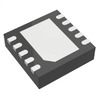
ADP2119ACPZ-3.3-R7 (1)

Manufacturer Part Number

ADP2119ACPZ-3.3-R7

Manufacturer

Analog Devices

Introduction

The ADP2119ACPZ-3.3-R7 is a step-down DC-DC switching regulator designed for efficient power management, specifically capable of converting input voltage ranging between 2.3V and 5.5V to a fixed output voltage of 3.3V.

Product Features and Performance

Step-Down Buck Regulator

Output Configuration: Positive

Topology: Buck

Output Type: Fixed

Single Output

Voltage - Input: 2.3V to 5.5V

Voltage - Output: 3.3V

Current - Output: 2A

Frequency - Switching: 1.2MHz

Synchronous Rectifier: Yes

Operating Temperature: -40°C to 125°C

Product Advantages

High Efficiency with Synchronous Rectification

Compact 10-LFCSP-WD (3x3) package suitable for space-constrained applications

High-frequency operation at 1.2MHz allows for smaller peripheral components

Key Technical Parameters

Min Input Voltage: 2.3V

Max Input Voltage: 5.5V

Fixed Output Voltage: 3.3V

Output Current: 2A

Switching Frequency: 1.2MHz

Operating Temperature Range: -40°C to 125°C

Quality and Safety Features

Designed for robust thermal performance and reliability within an operating temperature range of -40°C to 125°C

Compatibility

Surface Mount mounting type ensures compatibility with most PCB designs

Application Areas

Ideal for powering sensitive electronic devices in sectors like telecommunications, consumer electronics, and industrial systems

Product Lifecycle

Status: Active

This product is actively being manufactured and supplied, with no current indication of nearing discontinuation. Replacements or upgrades will be available as needed.

Several Key Reasons to Choose This Product

High efficiency and power density ensure minimal energy loss and reduced thermal footprint

Supports a wide range of input voltage, facilitating flexibility in power design

High-output current capacity suited for high-performance applications

Operates at a high switching frequency enabling the use of smaller, less costly capacitors and inductors

Robust operating temperature range guarantees performance in extreme conditions

Reliable and stable output with built-in synchronous rectification

Frequently Asked Questions(FAQ)

How does the ADP2119ACPZ-3.3-R7 compare to the ADP2114ACPZ-5.0-R7 in terms of output voltage and current capability for a 5V input system?
The ADP2119ACPZ-3.3-R7 delivers a fixed 3.3V output at up to 2A, making it suitable for applications requiring precise 3.3V rails from a 2.3V–5.5V input. In contrast, the ADP2114ACPZ-5.0-R7 provides a higher 5.0V output at the same 2A maximum, which is more appropriate when powering devices that operate closer to the input rail. While both use synchronous rectification and operate at 1.2MHz, the choice depends on the load’s voltage requirement and efficiency considerations across the input range.
What are the thermal implications of operating the ADP2119ACPZ-3.3-R7 at full 2A load with a 5.5V input in a compact 3x3mm package?
At 2A output and a 5.5V input, the ADP2119ACPZ-3.3-R7 experiences an approximate power dissipation of (5.5V - 3.3V) × 2A = 4.4W, though actual losses include switching and conduction inefficiencies. With only 4mm² of exposed pad area and minimal PCB copper, junction-to-ambient thermal resistance can exceed 40°C/W, leading to junction temperatures exceeding 120°C at ambient above 25°C. This necessitates careful layout with solid ground planes and thermal vias to maintain reliability within the -40°C to 125°C TJ rating.
Can the ADP2119ACPZ-3.3-R7 be used in battery-powered applications with Li-ion cells without additional filtering?
Yes, the ADP2119ACPZ-3.3-R7 supports direct connection to Li-ion cells (3.0V–4.2V nominal) down to its 2.3V minimum input. However, due to its 1.2MHz switching frequency, input capacitor selection must account for high-frequency ripple to avoid noise coupling into sensitive analog circuits. A low-ESR ceramic capacitor of at least 10µF should be placed close to the VIN pin, and output capacitors must meet ESR requirements to ensure stability under transient loads.
Why might the ADP2119ACPZ-3.3-R7 exhibit instability during fast load transients despite being a synchronous buck regulator?
Even with synchronous rectification, stability depends on output capacitance value, ESR, and loop compensation. The ADP2119ACPZ-3.3-R7 requires a minimum total output capacitance with ESR between 1mΩ and 50mΩ for phase margin optimization. Using ultra-low-ESR capacitors like X5R or X7R ceramics in parallel with a small tantalum or polymer capacitor helps dampen oscillations during sudden current changes, especially at light loads where control loop dynamics shift.
How does the 1.2MHz switching frequency of the ADP2119ACPZ-3.3-R7 affect PCB layout compared to lower-frequency regulators?
The 1.2MHz switching frequency allows smaller inductors and capacitors due to higher energy transfer per cycle, but it demands tighter PCB layout practices. Parasitic inductance in traces and vias can cause voltage spikes and EMI issues. Power paths (VIN, SW, GND) must be short and wide, and the SW node should avoid adjacent signal lines. Ground plane continuity beneath the IC is critical to minimize ground bounce and ensure stable operation.
Is external feedback required when using the ADP2119ACPZ-3.3-R7, and how does this impact system design complexity?
No external feedback resistors are needed because the ADP2119ACPZ-3.3-R7 has an internal feedback comparator set to 3.3V. This simplifies design and improves transient response by eliminating divider-induced delay. However, any modification to output voltage would require selecting a different part from the ADP2119 family, as fixed-output versions do not allow external adjustment.
What is the impact of operating the ADP2119ACPZ-3.3-R7 near its input voltage limits on efficiency and component stress?
When running at 5.5V input and 3.3V output, the duty cycle reaches approximately 58%, increasing conduction time and associated switch losses. Efficiency drops slightly due to higher gate drive and switching activity, but remains above 85% under typical conditions. Proximity to the 5.5V absolute maximum rating also increases stress on input protection diodes and capacitors, so input surge handling should be verified if used in environments with transient overvoltage risk.
How does the Moisture Sensitivity Level (MSL) of 3 for the ADP2119ACPZ-3.3-R7 influence manufacturing and storage procedures?
With an MSL of 3, the ADP2119ACPZ-3.3-R7 must be baked if stored beyond 168 hours (6.9 days) before reflow soldering to prevent popcorning during thermal cycling. Manufacturers should follow IPC/JEDEC J-STD-033 guidelines, including baking at 125°C for 24 hours and using moisture barrier bags with desiccant and humidity indicator cards. Proper handling ensures device integrity during assembly.
Can the ADP2119ACPZ-3.3-R7 replace linear regulators in space-constrained designs without compromising thermal performance?
Yes, the ADP2119ACPZ-3.3-R7 offers significant advantages over linear regulators in compact layouts. Its 3x3mm footprint and 2A capability eliminate the need for multiple parallel LDOs. Efficiency exceeds 80% even at light loads, reducing heat generation compared to LDOs dissipating (VIN - VOUT) × ILOAD. This makes it ideal for portable and industrial systems where size and thermal management are critical.
What precautions should be taken when paralleling the ADP2119ACPZ-3.3-R7 with other power stages in high-current applications?
Paralleling the ADP2119ACPZ-3.3-R7 is generally not recommended due to its fixed-frequency, single-phase architecture. Unequal load sharing can occur if devices have slight variations in threshold voltages or temperature coefficients. If used, external current balancing resistors or active load-sharing circuits are required, adding complexity and cost. Instead, designers should consider higher-current buck controllers compatible with multi-phase operation.
How does the synchronous rectifier topology in the ADP2119ACPZ-3.3-R7 improve efficiency compared to asynchronous designs?
The synchronous rectifier uses an internal MOSFET instead of a diode for the freewheeling path, reducing forward voltage drop and conduction losses—especially important at higher currents. For example, replacing a 0.5V Schottky diode with a 0.1V RDS(ON) MOSFET improves efficiency by ~2–5% at 2A load. This results in better thermal performance and longer battery life in portable applications powered by the ADP2119ACPZ-3.3-R7.
What role does the exposed pad play in the thermal performance of the ADP2119ACPZ-3.3-R7, and how should it be implemented in the PCB?
The exposed pad on the 10-LFCSP-WD package acts as a thermal interface to the PCB, significantly lowering junction-to-board thermal resistance. It should be connected to a large copper pour on the top layer and filled with thermal vias to inner or bottom-ground layers. Using 8–12 vias of 0.3mm diameter under the pad improves heat dissipation by 30–50%, enabling sustained operation at full 2A load without exceeding 125°C junction temperature.
Why might the ADP2119ACPZ-3.3-R7 not be suitable for automotive-grade applications despite its -40°C to 125°C operating range?
While the ADP2119ACPZ-3.3-R7 operates up to 125°C, it lacks AEC-Q100 qualification and robust fault protection features expected in automotive systems. Without functional safety mechanisms such as overtemperature lockout or input undervoltage hysteresis, it may fail unpredictably under harsh conditions. Automotive designs typically require parts validated for vibration, EMI immunity, and extended lifecycle support beyond standard commercial grades.
How does the cut tape and Digi-Reel packaging affect inventory management and automated assembly for the ADP2119ACPZ-3.3-R7?
Cut tape packaging suits low-volume prototyping, while Digi-Reel® format enables automated pick-and-place machines to feed components efficiently during mass production. Both formats comply with JEDEC standards, ensuring compatibility with industry-standard pick-and-place equipment. However, engineers must verify reel orientation and leader tape length to prevent misalignment during high-speed assembly of the 10-pin VFDFN package.
What are the implications of choosing ceramic output capacitors versus polymer types with the ADP2119ACPZ-3.3-R7?
Ceramic capacitors offer low ESR and high capacitance density, ideal for stable operation at 1.2MHz. However, their capacitance decreases significantly with DC bias, potentially causing instability if not derated properly. Polymer capacitors provide consistent capacitance under bias and better long-term reliability but are larger and more expensive. A hybrid approach—using one or two low-ESR ceramic caps plus one polymer cap—often yields optimal transient response and stability for the ADP2119ACPZ-3.3-R7.
Can the ADP2119ACPZ-3.3-R7 be used in solar-powered microcontrollers where input voltage varies from 2.8V to 4.5V?
Yes, the ADP2119ACPZ-3.3-R7 is well-suited for solar-powered MCUs with a 2.3V–5.5V input range. Its 1.2MHz switching minimizes inductor size, and synchronous rectification maximizes energy extraction from low-voltage panels. However, startup behavior must be tested under weak input conditions (<2.5V), as some MCUs draw microamps during boot-up, which could starve the regulator if quiescent current exceeds panel capability.
How does the fixed 3.3V output of the ADP2119ACPZ-3.3-R7 compare to adjustable alternatives in terms of bill of materials (BOM) cost and design simplicity?
The fixed 3.3V output eliminates the need for external feedback resistors, reducing BOM count and PCB real estate. Adjustable versions require two precision resistors, increasing cost and tolerance dependency. For the ADP2119ACPZ-3.3-R7, this simplification translates into faster time-to-market and fewer calibration steps, making it preferable when 3.3V is non-negotiable and load current is within 2A.
What steps should be taken to validate the ADP2119ACPZ-3.3-R7 in a prototype before committing to production?
Begin with a reference schematic matching the evaluation board layout, ensuring proper input/output decoupling and thermal via placement. Perform load transient tests at 0.5A and 2A, checking for overshoot and recovery time. Measure efficiency across input voltages and monitor junction temperature under worst-case conditions. Finally, conduct long-duration burn-in at elevated ambient temperatures to identify early failures related to solder joints or capacitor aging in the ADP2119ACPZ-3.3-R7 circuit.

Parts with Similar Specifications

The three parts on the right have similar specifications to Analog Devices Inc. ADP2119ACPZ-3.3-R7

Product Attribute ADP2119ACPZ-2.5-R7 ADP2119ACPZ-1.5-R7 ADP2119ACPZ-1.0-R7 ADP2120ACPZ-3.3-R7
Part Number ADP2119ACPZ-2.5-R7 ADP2119ACPZ-1.5-R7 ADP2119ACPZ-1.0-R7 ADP2120ACPZ-3.3-R7
Manufacturer Analog Devices Inc. Analog Devices Inc. Analog Devices Inc. Analog Devices Inc.
Base Product Number - DAC34H84 MAX500 ADS62P42
Operating Temperature - -40°C ~ 85°C 0°C ~ 70°C -40°C ~ 85°C
Voltage - Input (Max) - - - -
Output Type - Current - Unbuffered Voltage - Buffered -
Output Configuration - - - -
Frequency - Switching - - - -
Voltage - Input (Min) - - - -
Voltage - Output (Max) - - - -
Voltage - Output (Min/Fixed) - - - -
Function - - - -
Supplier Device Package - 196-NFBGA (12x12) 16-PDIP 64-VQFN (9x9)
Topology - - - -
Series - - - -
Current - Output - - - -
Package - Tape & Reel (TR) Tube Tape & Reel (TR)
Number of Outputs - - - -
Mounting Type - Surface Mount Through Hole Surface Mount
Synchronous Rectifier - - - -
Package / Case - 196-LFBGA 16-DIP (0.300', 7.62mm) 64-VFQFN Exposed Pad

ADP2119ACPZ-3.3-R7 Datasheet PDF

Download ADP2119ACPZ-3.3-R7 pdf datasheets and Analog Devices Inc. documentation for ADP2119ACPZ-3.3-R7 - Analog Devices Inc..

Datasheets
Cylindrical Battery Holders.pdf
PCN Assembly/Origin
2.73KHz.pdf
Other Related Documents
Tape and Reel Packaging.pdf

Customer Reviews

Evaluation: 10 Articles

  • Nath***rooks
    Jun 11, 2026

    Installed this power component in a converter board. Output remained stable under different load conditions and thermal performance was better than expected.

  • Dani***alkerTech
    Jun 1, 2026

    Product works, but setup took more effort than expected. Once configured the MCU ran reliably, although documentation support felt older compared with newer platforms. Fine for maintenance projects.

  • Yuki***aka88
    May 26, 2026

    信号通信プロジェクトでこのRS-485トランシーバーを使用しました。設置は簡単で、長距離ケーブルでも通信は安定していました。消費電力も、以前使用していたものより低くなっています。

  • Stev***aker
    May 20, 2026

    Solid diode for power rectification. Works well in switching circuits.

  • Bran***Lewis
    May 11, 2026

    Compact FPGA with good performance. Suitable for basic signal processing tasks.

  • Oliv***arris
    May 7, 2026

    Reliable I/O expander. Works well in embedded control applications.

  • Jess***Jones
    Apr 17, 2026

    It offers good value for the price, and the specifications match the description. I’ve been using it for two days with no issues, and I’ll definitely buy it again if I need it in the future.

  • Mich***Smith
    Apr 17, 2026

    Shipping was on time, the component pins are neatly aligned, and I tested 10 of them with a multimeter—all readings were within the specified range. Highly recommended.

  • Aman***arris
    Apr 3, 2026

    It was great—the entire process, from placing the order to receiving the package, went very smoothly. The components were consistent, the price was fair, and I had a very pleasant shopping experience.

  • Mike***nch
    Apr 3, 2026

    Better than expected! The resistance and capacitance readings were spot-on, and it passed the test on the first try. The service was reliable, and the packaging was thoughtful—I highly recommend it.

Write a Review

Your Email address will not be published.

Shipment

Delivery Time

In-stock items can be shipped within 24 hours. Some parts will be arranged for delivery within 1-2 days from the date all items arrive at our warehouse. And Allelco ships order once a day at about 17:00, except Sunday. Once the goods are shipped, the estimated delivery time depends on the shipping methods and Delivery destination. The table below shows are the logistic time for some common countries.

Delivery Cost

  1. Use your express account for shipment if you have one.
  2. Use our account for the shipment. Refer to the table below for the approximate charges.
(Different time frame / countries / package size has different price.)

Delivery Method

  1. Global Common Shipment by DHL / UPS / FedEx / TNT / EMS / SF we support.
  2. Others more shipping ways, please get in touch with your customer manager.

Common Countries Logistic Time Reference
Region Country Logistic Time(Day)
America United States 5
Brazil 7
Europe Germany 5
United Kingdom 4
Italy 5
Oceania Australia 6
New Zealand 5
Asia India 4
Japan 4
Middle East Israel 6
DHL & FedEx Shipment Charges Reference
Shipment charges(KG) Reference DHL(USD$)
0.00kg-1.00kg USD$30.00 - USD$60.00
1.00kg-2.00kg USD$40.00 - USD$80.00
2.00kg-3.00kg USD$50.00 - USD$100.00
Note:
The above table is for reference only. There may have some data bias for the uncontrollable factors.
Contact us if you have any questions.
  • QC (Quality Warranty)
  • Payment Support
  • Packaging
  • Certifications & Memberships

QC (Quality Warranty)

Allelco is committed to exceeding customer expectations through customer service excellence, order accuracy, and on-time delivery.
This is achieved through our commitment to the continual improvement of our processes, services, and products.


Strict quality inspection builds a solid foundation for electronic component quality.
  1. Visual inspection
  2. Performance testing and reliability verification
  3. Standardized full-process testing
  4. Precise control of every parameter
We eliminate defective components and ensure the stable operation of electronic devices through professional quality standards.

Payment Support

The payment method can be chosen from the methods shown below: Wire Transfer (T/T, Bank Transfer), Western Union, Credit card, PayPal.
  • HKBea
  • Paypal
  • MasterCard
  • Western-Union
  • VISA
Stable Delivery, Sincere Partnership — Your Faithful Supply Chain Partner
  • Efficient Supply Management
  • Cost-Saving Procurement
  • Fast Sourcing & Delivery
Contact us if you have any questions.

Packaging

Electrostatic Discharge Protection and Handling

All electrostatic-sensitive components are handled in accordance with electrostatic discharge control procedures. The products are hermetically sealed in anti-static safe packaging to prevent electrostatic damage. Appropriate labeling is also applied for identification and traceability. This ensures product integrity during storage, handling and transportation.


ESD

Certifications & Memberships

Third-party certified, strict quality control. Our certification
  • ISO 9001: 2015
  • ISO 13485: 2016
  • ISO 14001: 2015
  • ISO 28000: 2007
  • ISO 45001: 2018
  • GB/T 27922-2011
  • SMTA
  • IPC
  • ESD
  • PSMA
ADP2119ACPZ-3.3-R7 Image

ADP2119ACPZ-3.3-R7

Analog Devices Inc.
32D-ADP2119ACPZ-3.3-R7

Want a better price? Add to Cart and Submit RFQ now, we'll contact you immediately.

0 RFQ
Shopping cart (0 Items)
It is empty.
Compare List (0 Items)
It is empty.
Feedback

Your feedback matters! At Allelco, we value the user experience and strive to improve it constantly.
Please share your comments with us via our feedback form, and we'll respond promptly.
Thank you for choosing Allelco.

Subject
E-mail
Comments
Captcha
Drag or click to upload file
Upload File
types: .xls, .xlsx, .doc, .docx, .jpg, .png and .pdf.
Max file size: 10MB