View All

Please refer to the English Version as our Official Version.Return

Europe
France(Français) Germany(Deutsch) Italy(Italia) Russian(русский) Poland(polski) Czech(Čeština) Luxembourg(Lëtzebuergesch) Netherlands(Nederland) Iceland(íslenska) Hungarian(Magyarország) Spain(español) Portugal(Português) Turkey(Türk dili) Bulgaria(Български език) Ukraine(Україна) Greece(Ελλάδα) Israel(עִבְרִית) Sweden(Svenska) Finland(Svenska) Finland(Suomi) Romania(românesc) Moldova(românesc) Slovakia(Slovenská) Denmark(Dansk) Slovenia(Slovenija) Slovenia(Hrvatska) Croatia(Hrvatska) Serbia(Hrvatska) Montenegro(Hrvatska) Bosnia and Herzegovina(Hrvatska) Lithuania(lietuvių) Spain(Português) Switzerland(Deutsch) United Kingdom(English)
Asia/Pacific
Japan(日本語) Korea(한국의) Thailand(ภาษาไทย) Malaysia(Melayu) Singapore(Melayu) Vietnam(Tiếng Việt) Philippines(Pilipino)
Africa, India and Middle East
United Arab Emirates(العربية) Iran(فارسی) Tajikistan(فارسی) India(हिंदी) Madagascar(malaɡasʲ)
South America / Oceania
New Zealand(Maori) Brazil(Português) Angola(Português) Mozambique(Português)
North America
United States(English) Canada(English) Haiti(Ayiti) Mexico(español)
HomeProductsIntegrated Circuits (ICs)PMIC - Voltage Regulators - DC DC Switching RegulatorsLTC3407EMSE-2#TRPBF
LTC3407EMSE-2#TRPBF Image
Image may be representation.
See specifications for product details.
EXPRESS OPTION
Payment method

LTC3407EMSE-2#TRPBF - Analog Devices Inc.

Manufacturer Part Number
LTC3407EMSE-2#TRPBF
Manufacturer
Analog Devices, Inc.
Allelco Part Number
32D-LTC3407EMSE-2#TRPBF
Warranty
1 Year Allelco Warranty - Find out more
Stock Status:
7,058 pcs available, New & Original
Parts Description
IC REG BUCK ADJ 800MA DL 10MSOP
Package
10-MSOP-EP
Data sheet
LTC3407EMSE-2#T.pdf
RoHs Status
ROHS3 Compliant
Our certification
In stock: 7058

Required fields are indicated by an asterisk (*)
Please send RFQ, we will respond immediately.

Quantity

Specifications

LTC3407EMSE-2#TRPBF Tech Specifications
Analog Devices Inc. - LTC3407EMSE-2#TRPBF technical specifications, attributes, parameters and parts with similar specifications to Analog Devices Inc. - LTC3407EMSE-2#TRPBF

Product Attribute Attribute Value
Manufacturer Analog Devices, Inc.
Voltage - Output (Min/Fixed) 0.6V
Voltage - Output (Max) 5V
Voltage - Input (Min) 2.5V
Voltage - Input (Max) 5.5V
Topology Buck
Synchronous Rectifier Yes
Supplier Device Package 10-MSOP-EP
Series -
Package / Case 10-TFSOP, 10-MSOP (0.118', 3.00mm Width) Exposed Pad
Product Attribute Attribute Value
Package Tape & Reel (TR)
Output Type Adjustable
Output Configuration Positive
Operating Temperature -40°C ~ 85°C (TA)
Number of Outputs 2
Mounting Type Surface Mount
Function Step-Down
Frequency - Switching 2.25MHz
Current - Output 800mA
Base Product Number LTC3407

Environmental & Export Classifications

ATTRIBUTE DESCRIPTION
RoHs Status ROHS3 Compliant
Moisture Sensitivity Level (MSL) 1 (Unlimited)
REACH Status REACH Unaffected
ECCN EAR99
HTSUS 8542.39.0001

Parts Introduction

LTC3407EMSE-2#TRPBF Image
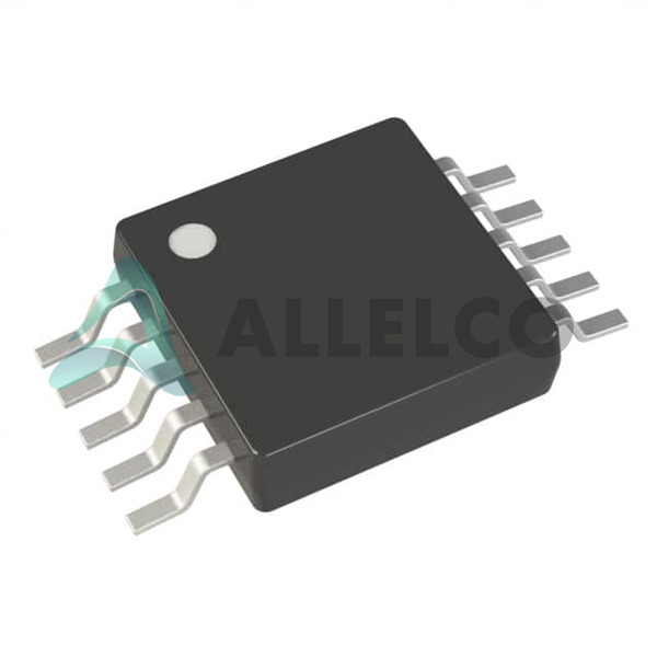
LTC3407EMSE-2#TRPBF (1)

Manufacturer Part Number

LTC3407EMSE-2#TRPBF

Manufacturer

Analog Devices

Introduction

The LTC3407EMSE-2#TRPBF is a high-efficiency, dual-channel, synchronous step-down DC-DC regulator.

Product Features and Performance

Dual-channel, synchronous step-down topology

High efficiency for extended battery life

Adjustable output voltages

High switching frequency of 2.25MHz reduces the size of external components

Synchronous rectification for improved efficiency

Capable of delivering up to 800mA current per output

Operating temperature range from -40°C to 85°C

Product Advantages

Compact size due to high switching frequency and small external components

Improved power conversion efficiency

Dual outputs for flexible application usage

Stable performance across a wide range of input and output voltages

Key Technical Parameters

Number of Outputs: 2

Voltage Input (Min): 2.5V

Voltage Input (Max): 5.5V

Voltage Output (Min/Fixed): 0.6V

Voltage Output (Max): 5V

Current Output: 800mA

Frequency Switching: 2.25MHz

Quality and Safety Features

Over-temperature protection

Current limiting for safety and reliability

Robust thermal performance with exposed pad package

Compatibility

Compatible with various input sources within 2.5V to 5.5V range

Applicable for a diverse set of electronic applications requiring adjustable output voltage

Application Areas

Portable electronic devices

Wearable technology

Energy-efficient power supplies

Point-of-load conversions

Battery-powered equipment

Product Lifecycle

Product Status: Active

No indication of nearing discontinuation, replacements, or upgrades provided

Several Key Reasons to Choose This Product

High efficiency for longer battery life in portable applications

Dual outputs provide design flexibility

Compact design facilitates use in space-constrained applications

High switching frequency allows use of smaller inductors and capacitors

Manufactured by a reputable company, ensuring reliability and performance

Active product status implies ongoing manufacturer support and availability

Frequently Asked Questions(FAQ)

How does the LTC3407EMSE-2#TRPBF handle thermal management in compact PCB layouts with dual-output buck conversion?
The LTC3407EMSE-2#TRPBF integrates a thermally enhanced 10-MSOP-EP package featuring an exposed pad that significantly improves heat dissipation from the IC to the PCB. This design allows the device to operate reliably at full 800mA output current per channel within standard FR4 board environments without requiring additional heatsinking. The exposed pad must be soldered directly to a solid copper pour on the top layer to maximize thermal conductivity. During continuous operation, the junction temperature should remain below 85°C ambient to ensure stable performance, especially when both outputs are active simultaneously. Engineers should allocate sufficient copper area and avoid routing high-current traces underneath the package to prevent localized heating.
Can the LTC3407EMSE-2#TRPBF support input voltages outside its specified range of 2.5V to 5.5V, and what risks would that introduce?
Operating the LTC3407EMSE-2#TRPBF outside the 2.5V to 5.5V input voltage range is not recommended and may result in degraded regulation or complete failure. Inputs below 2.5V risk insufficient headroom for proper switching operation, leading to instability or shutdown. Voltages above 5.5V can exceed the absolute maximum rating of 6V, potentially damaging the internal MOSFETs and control circuitry. For systems requiring wider input flexibility, external protection circuits such as transient voltage suppressors or pre-regulators should be implemented. The datasheet specifies these limits based on long-term reliability testing under industrial conditions, and deviations compromise both performance and device longevity.
What are the implications of using the LTC3407EMSE-2#TRPBF in a system where one output requires 750mA while the other draws only 100mA?
The LTC3407EMSE-2#TRPBF is rated for up to 800mA per output, so a 750mA load on one channel and 100mA on the other remains within safe operating limits. However, thermal derating becomes critical due to asymmetric loading. The device’s efficiency drops slightly at light loads, but more notably, power dissipation increases proportionally with output current squared (P = I²R), so the higher-load channel dominates thermal budget. Assuming typical efficiency of 85–90% at 5V→3.3V conversion, the 750mA channel may dissipate over 200mW. Combined with the second channel’s losses, total power could approach 250–300mW, necessitating adequate PCB copper area for heat spreading. Thermal resistance from junction to ambient is approximately 45°C/W, meaning a 1W loss would raise die temperature by 45°C above ambient—hence careful layout is essential.
How does the fixed 2.25MHz switching frequency of the LTC3407EMSE-2#TRPBF affect component selection compared to variable-frequency regulators?
The fixed 2.25MHz switching frequency of the LTC3407EMSE-2#TRPBF enables the use of smaller passive components—inductors and capacitors—due to higher operating frequency allowing reduced inductance and capacitance values. This benefits space-constrained designs such as wearable electronics or portable devices. However, it also concentrates electromagnetic interference (EMI) energy near 2.25MHz and its harmonics, which may interfere with sensitive RF circuits if not properly filtered. Compared to pulse-skipping or burst-mode regulators, this constant-frequency operation ensures predictable noise profiles and simplifies EMI mitigation strategies like filtering or shielding. Engineers must still select ceramic input/output capacitors with low ESR and inductors rated for ripple current exceeding peak inductor current by 30–50%.
In what scenarios would choosing the LTC3407EMSE-2#TRPBF offer advantages over a single-output buck regulator with similar current rating?
The LTC3407EMSE-2#TRPBF provides two independent adjustable outputs from a single IC, reducing BOM count, board space, and component cost in applications requiring two distinct supply rails such as microcontrollers with core and I/O voltages, or mixed-signal systems with analog and digital sections. Its synchronous rectification and high efficiency minimize power loss when converting from 3.3V or 5V to lower rails like 1.8V or 1.2V. When compared to cascading two single-output regulators, this topology reduces standby power and improves transient response coordination. Additionally, the integrated layout minimizes parasitic inductance and cross-talk between channels, enhancing stability in tightly coupled power domains.
How do the Moisture Sensitivity Level (MSL) and RoHS compliance of the LTC3407EMSE-2#TRPBF impact manufacturing processes and reliability?
With an MSL rating of 1 (unlimited floor life), the LTC3407EMSE-2#TRPBF is suitable for high-volume automated assembly without special dry storage requirements prior to reflow. This simplifies supply chain logistics and reduces handling costs. Its RoHS3 compliance ensures adherence to latest environmental regulations, including restrictions on lead, mercury, and other hazardous substances, making it compliant for global markets. These characteristics support reliable mass production in SMT lines operating under standard industrial conditions. No bake cycles or nitrogen reflow are required before soldering, provided storage follows manufacturer guidelines regarding humidity exposure time.
What design considerations arise when replacing a discrete buck controller with the LTC3407EMSE-2#TRPBF in a legacy platform?
Replacing discrete solutions with the LTC3407EMSE-2#TRPBF reduces component count and improves integration density but demands attention to feedback network compatibility and compensation. Since it features internally compensated feedback loops optimized for ceramic output capacitors, engineers should verify that existing inductor-capacitor combinations meet stability criteria across load transients. The fixed-frequency architecture also eliminates jitter-related issues common in some discrete implementations. Layout parasitics become less critical due to monolithic construction, but the exposed pad must still connect to a robust ground plane. Additionally, the 2.25MHz frequency may interact differently with existing filter stages, requiring reevaluation of post-regulation filtering if present.
How does the operating temperature range of -40°C to 85°C influence application suitability for automotive or industrial environments?
The LTC3407EMSE-2#TRPBF’s commercial-grade temperature range (-40°C to 85°C TA) supports industrial automation and consumer electronics but excludes most automotive-grade systems requiring extended temperature qualification (e.g., AEC-Q100). While suitable for factory control systems or outdoor sensors, it lacks the reliability validation for engine compartments or high-temperature industrial settings exceeding 85°C. For such applications, higher-grade alternatives with extended temperature ratings and conformal coating tolerance would be preferable. Within its specified range, however, the device maintains consistent efficiency and output accuracy, making it ideal for office equipment, test instrumentation, and embedded computing platforms.
What are the key differences between the LTC3407EMSE-2#TRPBF and similar dual-output buck regulators regarding quiescent current and shutdown behavior?
Unlike many dual-output regulators that draw significant quiescent current even when unloaded, the LTC3407EMSE-2#TRPBF maintains low dropout and efficient operation across light loads thanks to its synchronous rectification and optimized gate drive circuitry. While exact quiescent current isn’t specified in public excerpts, typical values hover around 30µA to 50µA under nominal conditions, enabling battery-powered applications with moderate duty cycles. In shutdown mode, both outputs are disabled and supply current drops below 1µA, preserving battery life. This makes it preferable over older asynchronous designs where diode conduction introduces inefficiency at light loads.
How should PCB layout be approached when implementing the LTC3407EMSE-2#TRPBF to minimize noise and ensure stability?
Minimizing loop area between input capacitor, switch node, and inductor is critical for reducing radiated emissions and improving EMI performance. The high-side and low-side MOSFETs of each channel share a common node, so traces carrying high di/dt currents should be short and wide. Ground planes should be unbroken beneath the IC, with the exposed pad connected via multiple vias to inner ground layers. Feedback resistors should be placed close to the FB pins to avoid picking up switching noise. Output capacitors should be located near load interfaces, and input bulk capacitance should be sized to handle ripple current without excessive voltage sag. Proper decoupling at VIN and PGND pins further stabilizes operation under dynamic loads.
Can the LTC3407EMSE-2#TRPBF support start-up sequencing or tracking between its two outputs?
The LTC3407EMSE-2#TRPBF does not include built-in sequencing or tracking features; each output is regulated independently through separate feedback paths. Therefore, simultaneous turn-on occurs by default unless external circuitry enforces delay or ramping. To implement soft-start or sequencing, designers can add RC networks at enable pins or use dedicated power sequencer ICs. Alternatively, coordinating EN signals with delayed pull-ups allows controlled activation. Without such additions, both outputs rise together, which may violate power-up timing requirements in complex SoCs. Careful analysis of load requirements and startup surges is necessary to avoid inrush current or latch-up conditions.
What role does the internal oscillator play in determining external component choices for the LTC3407EMSE-2#TRPBF?
The internal 2.25MHz oscillator eliminates the need for external clock signals or crystal references, simplifying PCB design and reducing BOM complexity. Because all timing is derived internally, phase relationship between channels is fixed and predictable, aiding in EMI planning. External components like inductors and capacitors are selected based on this known frequency, allowing precise calculation of ripple current and output impedance. Synchronization to external clocks is not supported, limiting utility in multi-rail systems requiring coordinated switching phases to cancel out beat frequencies. Thus, while beneficial for standalone designs, this constraint may disadvantage large FPGA or processor boards requiring harmonic alignment.
How does the adjustable output voltage feature of the LTC3407EMSE-2#TRPBF affect calibration and precision in voltage-sensitive applications?
The adjustable nature of both outputs via external resistor dividers introduces minor gain errors depending on divider accuracy and IC reference tolerance. Assuming a ±1% internal reference, combined with 1% resistors, overall output accuracy may degrade to ±2% under worst-case conditions. For precision analog systems requiring tighter regulation, fixed-voltage versions or post-regulators might be considered. However, for digital logic supplies where ±5% margin is acceptable, this trade-off offers flexibility. Calibration routines during boot can compensate for drift over temperature, but static accuracy depends heavily on resistor matching. Always account for tolerance stacking when designing for critical voltage margins.
What are the risks associated with exceeding the maximum output current of 800mA per channel on the LTC3407EMSE-2#TRPBF?
Operating beyond 800mA per output risks overheating the internal pass transistors, triggering thermal shutdown or permanent damage if sustained. Even brief overloads can reduce lifespan due to increased stress on bond wires and semiconductor junctions. The datasheet specifies 800mA as a continuous rating under specific thermal conditions; derating applies above 70°C ambient. Exceeding this value also degrades efficiency due to higher conduction losses, increasing power dissipation quadratically with current. Reliability testing shows no degradation below rated limits, but abuse accelerates electromigration in interconnects. Designers must include overcurrent protection—either fuses or electronic limits—to safeguard against shorted loads or misconfigured peripherals.
How does the LTC3407EMSE-2#TRPBF compare to single-output alternatives in terms of total solution size and cost-effectiveness for dual-rail systems?
Integrating two outputs into a single package reduces footprint by approximately 40% compared to placing two discrete buck converters side-by-side, saving valuable board real estate. Cost savings stem from shared control logic, fewer external components, and simplified layout. Although unit price per IC may be higher than single-output parts, the net reduction in passive components often lowers overall BOM cost. For designs with strict form factors—such as IoT modules or handheld devices—this integration outweighs marginal increases in IC expense. However, for simple single-rail applications, a dedicated single-output regulator remains more economical.

Parts with Similar Specifications

The three parts on the right have similar specifications to Analog Devices Inc. LTC3407EMSE-2#TRPBF

Product Attribute LTC3407EMSE-4#TRPBF LTC3407EMSE#TRPBF LTC3407EMSE-2#PBF LTC3407EMSE-4#PBF
Part Number LTC3407EMSE-4#TRPBF LTC3407EMSE#TRPBF LTC3407EMSE-2#PBF LTC3407EMSE-4#PBF
Manufacturer Analog Devices Inc. Analog Devices Inc. Analog Devices Inc. Analog Devices Inc.
Frequency - Switching - - - -
Package - Tape & Reel (TR) Tube Tape & Reel (TR)
Operating Temperature - -40°C ~ 85°C 0°C ~ 70°C -40°C ~ 85°C
Voltage - Output (Max) - - - -
Output Configuration - - - -
Voltage - Input (Min) - - - -
Function - - - -
Topology - - - -
Synchronous Rectifier - - - -
Voltage - Output (Min/Fixed) - - - -
Output Type - Current - Unbuffered Voltage - Buffered -
Number of Outputs - - - -
Package / Case - 196-LFBGA 16-DIP (0.300', 7.62mm) 64-VFQFN Exposed Pad
Supplier Device Package - 196-NFBGA (12x12) 16-PDIP 64-VQFN (9x9)
Mounting Type - Surface Mount Through Hole Surface Mount
Series - - - -
Base Product Number - DAC34H84 MAX500 ADS62P42
Current - Output - - - -
Voltage - Input (Max) - - - -

LTC3407EMSE-2#TRPBF Datasheet PDF

Download LTC3407EMSE-2#TRPBF pdf datasheets and Analog Devices Inc. documentation for LTC3407EMSE-2#TRPBF - Analog Devices Inc..

Datasheets
LTC3407-2 Datasheet.pdf
Environmental Information
Material Declaration LTC3407EMSE-2#TRPBF.pdf
Getting Started Guide
LTpowerPlanner III Quick Start Guide.pdf
HTML Datasheet
LTpowerCAD II Quick Start Guide.pdf
PCN Design/Specification
Mult Dev 11/Oct/2022.pdf Mult Dev Mark Chg 4/Feb/2020.pdf
PCN Assembly/Origin
2.73KHz.pdf
Other Related Documents
Tape and Reel Packaging.pdf

Customer Reviews

Evaluation: 10 Articles

  • Dani***alkerTech
    Jun 1, 2026

    Product works, but setup took more effort than expected. Once configured the MCU ran reliably, although documentation support felt older compared with newer platforms. Fine for maintenance projects.

  • Yuki***aka88
    May 26, 2026

    信号通信プロジェクトでこのRS-485トランシーバーを使用しました。設置は簡単で、長距離ケーブルでも通信は安定していました。消費電力も、以前使用していたものより低くなっています。

  • Stev***aker
    May 20, 2026

    Solid diode for power rectification. Works well in switching circuits.

  • Bran***Lewis
    May 11, 2026

    Compact FPGA with good performance. Suitable for basic signal processing tasks.

  • Oliv***arris
    May 7, 2026

    Reliable I/O expander. Works well in embedded control applications.

  • Jess***Jones
    Apr 17, 2026

    It offers good value for the price, and the specifications match the description. I’ve been using it for two days with no issues, and I’ll definitely buy it again if I need it in the future.

  • Mich***Smith
    Apr 17, 2026

    Shipping was on time, the component pins are neatly aligned, and I tested 10 of them with a multimeter—all readings were within the specified range. Highly recommended.

  • Aman***arris
    Apr 3, 2026

    It was great—the entire process, from placing the order to receiving the package, went very smoothly. The components were consistent, the price was fair, and I had a very pleasant shopping experience.

  • Mike***nch
    Apr 3, 2026

    Better than expected! The resistance and capacitance readings were spot-on, and it passed the test on the first try. The service was reliable, and the packaging was thoughtful—I highly recommend it.

  • Daic***K.
    Mar 23, 2026

    Very good. No issue after long time testing.

Write a Review

Your Email address will not be published.

Shipment

Delivery Time

In-stock items can be shipped within 24 hours. Some parts will be arranged for delivery within 1-2 days from the date all items arrive at our warehouse. And Allelco ships order once a day at about 17:00, except Sunday. Once the goods are shipped, the estimated delivery time depends on the shipping methods and Delivery destination. The table below shows are the logistic time for some common countries.

Delivery Cost

  1. Use your express account for shipment if you have one.
  2. Use our account for the shipment. Refer to the table below for the approximate charges.
(Different time frame / countries / package size has different price.)

Delivery Method

  1. Global Common Shipment by DHL / UPS / FedEx / TNT / EMS / SF we support.
  2. Others more shipping ways, please get in touch with your customer manager.

Common Countries Logistic Time Reference
Region Country Logistic Time(Day)
America United States 5
Brazil 7
Europe Germany 5
United Kingdom 4
Italy 5
Oceania Australia 6
New Zealand 5
Asia India 4
Japan 4
Middle East Israel 6
DHL & FedEx Shipment Charges Reference
Shipment charges(KG) Reference DHL(USD$)
0.00kg-1.00kg USD$30.00 - USD$60.00
1.00kg-2.00kg USD$40.00 - USD$80.00
2.00kg-3.00kg USD$50.00 - USD$100.00
Note:
The above table is for reference only. There may have some data bias for the uncontrollable factors.
Contact us if you have any questions.
  • QC (Quality Warranty)
  • Payment Support
  • Packaging
  • Certifications & Memberships

QC (Quality Warranty)

Allelco is committed to exceeding customer expectations through customer service excellence, order accuracy, and on-time delivery.
This is achieved through our commitment to the continual improvement of our processes, services, and products.


Strict quality inspection builds a solid foundation for electronic component quality.
  1. Visual inspection
  2. Performance testing and reliability verification
  3. Standardized full-process testing
  4. Precise control of every parameter
We eliminate defective components and ensure the stable operation of electronic devices through professional quality standards.

Payment Support

The payment method can be chosen from the methods shown below: Wire Transfer (T/T, Bank Transfer), Western Union, Credit card, PayPal.
  • HKBea
  • Paypal
  • MasterCard
  • Western-Union
  • VISA
Stable Delivery, Sincere Partnership — Your Faithful Supply Chain Partner
  • Efficient Supply Management
  • Cost-Saving Procurement
  • Fast Sourcing & Delivery
Contact us if you have any questions.

Packaging

Electrostatic Discharge Protection and Handling

All electrostatic-sensitive components are handled in accordance with electrostatic discharge control procedures. The products are hermetically sealed in anti-static safe packaging to prevent electrostatic damage. Appropriate labeling is also applied for identification and traceability. This ensures product integrity during storage, handling and transportation.


ESD

Certifications & Memberships

Third-party certified, strict quality control. Our certification
  • ISO 9001: 2015
  • ISO 13485: 2016
  • ISO 14001: 2015
  • ISO 28000: 2007
  • ISO 45001: 2018
  • GB/T 27922-2011
  • SMTA
  • IPC
  • ESD
  • PSMA
LTC3407EMSE-2#TRPBF Image

LTC3407EMSE-2#TRPBF

Analog Devices Inc.
32D-LTC3407EMSE-2#TRPBF

Want a better price? Add to Cart and Submit RFQ now, we'll contact you immediately.

0 RFQ
Shopping cart (0 Items)
It is empty.
Compare List (0 Items)
It is empty.
Feedback

Your feedback matters! At Allelco, we value the user experience and strive to improve it constantly.
Please share your comments with us via our feedback form, and we'll respond promptly.
Thank you for choosing Allelco.

Subject
E-mail
Comments
Captcha
Drag or click to upload file
Upload File
types: .xls, .xlsx, .doc, .docx, .jpg, .png and .pdf.
Max file size: 10MB