
Manufacturer Part Number
AD9633BCPZ-125
Manufacturer
analog-devices
Introduction
The AD9633 is a high-performance, low power, quad-channel, 12-bit, 125 MSPS analog-to-digital converter (ADC) with integrated sample-and-hold amplifiers. It features simultaneous sampling on all four channels, low power consumption, and a compact, low-profile package. The AD9633 is ideal for a wide range of applications including medical imaging, communications, and industrial instrumentation.
Product Features and Performance
12-bit resolution
125 MSPS sampling rate
4 differential analog inputs
Integrated sample-and-hold amplifiers
Simultaneous sampling on all 4 channels
Low power consumption
Compact 48-pin WFQFN package
Product Advantages
Excellent dynamic performance with low power
Simultaneous sampling of all 4 channels
Integrated sample-and-hold amplifiers
Wide operating temperature range of -40°C to 85°C
Key Reasons to Choose this Product
High-performance, cost-effective solution for multi-channel data acquisition
Compact package and low power consumption make it ideal for space-constrained applications
Robust design and wide operating temperature range ensure reliable operation in demanding environments
Proven performance and reliability from a trusted manufacturer, Analog Devices
Quality and Safety Features
Manufactured in ISO certified facilities
Rigorous testing and quality control processes
RoHS and REACH compliant
Compatibility
The AD9633 is compatible with a wide range of digital signal processors, microcontrollers, and other data acquisition systems.
Application Areas
Medical imaging equipment
Communications systems
Industrial instrumentation
Test and measurement equipment
Product Lifecycle
The AD9633 is an active product. There are no immediate plans for discontinuation. Alternative models with similar performance and features include the AD9634 and AD9637 series. If you have any questions or need assistance, please contact our sales team through our website.
 AD9632AR-REEL7Analog Devices Inc.IC OPAMP VF ULDIST 70MA 8SOIC
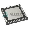 AD9633BCPZRL7-80Analog Devices Inc.IC ADC 12BIT PIPELINED 48LFCSP
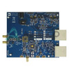 AD9634-250EBZAnalog Devices Inc.BOARD EVAL FOR AD9634 250MSPS
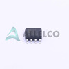 AD9632ARZ-REEL7Analog Devices Inc.IC VOLTAGE FEEDBACK 1 CIRC 8SOIC
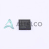 AD9634BCPZ-170Analog Devices Inc.IC ADC 12BIT PIPELINED 32LFCSP
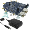 AD9633-125EBZAnalog Devices Inc.BOARD EVAL FOR AD9633
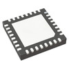 AD9634BCPZ-210Analog Devices Inc.IC ADC 12BIT PIPELINED 32LFCSP
 AD9634-210EBZAnalog Devices Inc.BOARD EVAL FOR AD9634 210MSPS


