
Manufacturer Part Number
ADG5421FBCPZ-RL7
Manufacturer
analog-devices
Introduction
The ADG5421FBCPZ-RL7 is a high-performance, dual single-pole, single-throw (SPST) analog switch from Analog Devices. This switch offers exceptional performance with fast switching times, low on-resistance, and high bandwidth, making it suitable for a wide range of applications, including data acquisition, instrumentation, and signal routing.
Product Features and Performance
Dual SPST analog switch
Very low on-resistance (14Ω max)
Excellent channel-to-channel matching (20mΩ)
Fast switching times (15.9μs max turn-on, 160ns max turn-off)
High bandwidth (-3dB at 630MHz)
Low charge injection (-150pC)
Low channel capacitance (6pF off, 5pF off)
Extremely low leakage current (200pA max)
Excellent crosstalk performance (-78dB @ 1MHz)
Wide supply voltage range (8V to 44V single, ±5V to ±22V dual)
Extended operating temperature range (-40°C to 125°C)
Product Advantages
Exceptional RF and analog performance
Compact, space-saving 10-WFDFN, CSP package
Versatile single and dual supply voltage options
Suitable for a wide range of applications
Key Reasons to Choose This Product
Industry-leading performance for high-speed, high-precision signal switching
Compact and power-efficient design for space-constrained applications
Robust operating temperature range for use in demanding environments
Reliable and long-lasting solution backed by Analog Devices' reputation
Quality and Safety Features
Manufactured to the highest quality standards
RoHS-compliant and lead-free
Compatibility
The ADG5421FBCPZ-RL7 is compatible with a wide range of electronic systems and can be used in various applications.
Application Areas
Data acquisition systems
Instrumentation and test equipment
Signal routing and switching
RF and analog signal processing
Multiplexing and demultiplexing
Product Lifecycle
The ADG5421FBCPZ-RL7 is an active product, and there are no known plans for discontinuation. While there may be equivalent or alternative models available from Analog Devices or other manufacturers, it is recommended to contact our website's sales team for the most up-to-date information on available options.
 ADG5421BRMZAnalog Devices
 ADG5419BRMZ-RL7Analog Devices Inc.IC SWITCH SPDT X 1 14OHM 8MSOP
 ADG5421BRMZ-RL7Analog Devices Inc.IC SWITCH SPST-NOX2 14OHM 10MSOP
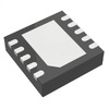 ADG5421BCPZ-RL7Analog Devices Inc.IC SW SPST-NOX2 14OHM 10LFCSP
 ADG5419BRMZAnalog Devices Inc.IC SWITCH SPDT X 1 14OHM 8MSOP
 ADG5433BRUZAnalog Devices Inc.IC SWITCH SPDT X 3 14OHM 16TSSOP
 ADG5433BRUZ-REEL7Analog Devices
 ADG5423BRMZ-RL7Analog Devices Inc.IC SWITCH SPST-NOX2 14OHM 10MSOP
 ADG5433WBRUZAnalog Devices Inc.IC SWITCH SPDT X 3 14OHM 16TSSOP
 ADG5419BCPZ-RL7Analog Devices Inc.IC SWITCH SPDT X 1 14OHM 8LFCSP
 ADG5423BRMZ-RADI (Analog Devices, Inc.)


