View All

Please refer to the English Version as our Official Version.Return

Europe
France(Français) Germany(Deutsch) Italy(Italia) Russian(русский) Poland(polski) Czech(Čeština) Luxembourg(Lëtzebuergesch) Netherlands(Nederland) Iceland(íslenska) Hungarian(Magyarország) Spain(español) Portugal(Português) Turkey(Türk dili) Bulgaria(Български език) Ukraine(Україна) Greece(Ελλάδα) Israel(עִבְרִית) Sweden(Svenska) Finland(Svenska) Finland(Suomi) Romania(românesc) Moldova(românesc) Slovakia(Slovenská) Denmark(Dansk) Slovenia(Slovenija) Slovenia(Hrvatska) Croatia(Hrvatska) Serbia(Hrvatska) Montenegro(Hrvatska) Bosnia and Herzegovina(Hrvatska) Lithuania(lietuvių) Spain(Português) Switzerland(Deutsch) United Kingdom(English)
Asia/Pacific
Japan(日本語) Korea(한국의) Thailand(ภาษาไทย) Malaysia(Melayu) Singapore(Melayu) Vietnam(Tiếng Việt) Philippines(Pilipino)
Africa, India and Middle East
United Arab Emirates(العربية) Iran(فارسی) Tajikistan(فارسی) India(हिंदी) Madagascar(malaɡasʲ)
South America / Oceania
New Zealand(Maori) Brazil(Português) Angola(Português) Mozambique(Português)
North America
United States(English) Canada(English) Haiti(Ayiti) Mexico(español)
HomeProductsIntegrated Circuits (ICs)Memory - Configuration Proms for FPGAsXC18V512VQ44C
XC18V512VQ44C Image
Image may be representation.
See specifications for product details.
EXPRESS OPTION
Payment method

XC18V512VQ44C - AMD

Manufacturer Part Number
XC18V512VQ44C
Manufacturer
AMD Xilinx
Allelco Part Number
32D-XC18V512VQ44C
Warranty
1 Year Allelco Warranty - Find out more
Stock Status:
6,000 pcs available, New & Original
Parts Description
IC PROM SRL CONFIG 512K 44-VQFP
Package
44-VQFP (10x10)
Data sheet
XC18V512VQ44C.pdf

HTML Datasheet

XC18V00 Series.pdf

PCN Part Status Change

2.73KHz.pdf

Environmental Information

Xilinx REACH211 Cert.pdf
RoHs Status
 
Our certification
In stock: 6000
  • Unit Price: $23.47
  • Subtotal: $0.00

Want a better price?
Add to Cart and Submit RFQ now, we'll contact you immediately.

Quantity Unit Price Ext. Price
1+ $23.47 $23.47
200+ $9.08 $1,816.00
500+ $8.76 $4,380.00
1000+ $8.61 $8,610.00
The above prices does not include taxes and freight rates, which will be calculated on the order pages.

Specifications

XC18V512VQ44C Tech Specifications
AMD - XC18V512VQ44C technical specifications, attributes, parameters and parts with similar specifications to AMD - XC18V512VQ44C

Product Attribute Attribute Value
Manufacturer AMD Xilinx
Voltage - Supply 3V ~ 3.6V
Supplier Device Package 44-VQFP (10x10)
Series -
Programmable Type In System Programmable
Package / Case 44-TQFP
Product Attribute Attribute Value
Package Tray
Operating Temperature 0°C ~ 70°C
Mounting Type Surface Mount
Memory Size 512kb
Base Product Number XC18V512

Environmental & Export Classifications

ATTRIBUTE DESCRIPTION
RoHs Status RoHS non-compliant
Moisture Sensitivity Level (MSL) 3 (168 Hours)
REACH Status REACH Unaffected
ECCN 3A991B1B2
HTSUS 8542.32.0071

Parts Introduction

XC18V512VQ44C Image
XC18V512VQ44C (1)

Manufacturer Part Number

XC18V512VQ44C

Manufacturer

Xilinx

Introduction

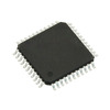
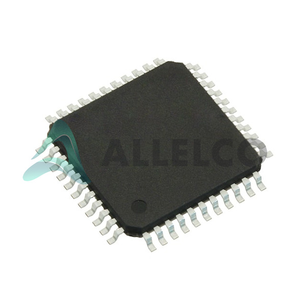
The XC18V512VQ44C is a Memory Configuration PROM designed for configuring Xilinx FPGAs with a memory size of 512kb.

Product Features and Performance

In System Programmable

Memory Size of 512kb

Operating Temperature Range of 0°C to 70°C

Surface Mount Technology

Packaged in a 44-VQFP (10x10)

Product Advantages

Designed specifically for FPGA configuration

Reliable data storage for system boot-up configurations

Key Technical Parameters

Memory Size: 512kb

Voltage - Supply: 3V ~ 3.6V

Operating Temperature: 0°C ~ 70°C

Package / Case: 44-TQFP

Quality and Safety Features

Robust construction designed for optimal performance within specified temperature range

Compatibility

Compatible with Xilinx FPGA devices for configuration purposes

Application Areas

Used in FPGA-based applications across various industries such as telecommunications, automotive, and consumer electronics

Product Lifecycle

Obsolete status

No direct replacements or upgrades specified

Several Key Reasons to Choose This Product

Optimal solution for Xilinx FPGA configuration

Compact and efficient with a 44-TQFP packaging

Supports a voltage supply range from 3V to 3.6V

Designed to function within a standard operating temperature range suitable for most industrial applications

Legacy support for existing systems using Xilinx FPGA technology

Frequently Asked Questions(FAQ)

How does the XC18V512VQ44C compare to the AT17LV512-10CC in terms of voltage tolerance and maximum operating frequency, and what are the implications for power-sensitive embedded designs?
The XC18V512VQ44C operates over a supply range of 3.0V to 3.6V with an industrial-grade temperature specification, while the AT17LV512-10CC supports 2.7V to 3.6V and is rated for commercial operation up to 10 MHz. Given that both devices target serial configuration memory roles, the tighter voltage margin of the XC18V512VQ44C may offer better stability in noisy environments, though it lacks the lower-voltage efficiency advantage of the AT17LV512-10CC. Designers must consider whether the extended reliability features justify the slightly higher power envelope in applications where battery life or thermal constraints dominate.
What is the significance of the Moisture Sensitivity Level (MSL) rating of 3 for the XC18V512VQ44C, and how should assembly personnel handle this component during PCB manufacturing?
The MSL 3 classification indicates the XC18V512VQ44C requires baking if exposed to ambient humidity beyond 168 hours after opening its moisture barrier bag. This precaution prevents popcorning during reflow soldering due to trapped moisture vaporizing rapidly at peak temperatures. Assembly teams must adhere to JEDEC J-STD-033 guidelines—typically storing parts in dry cabinets below 10% relative humidity and baking at 125°C for 24–48 hours before use—to avoid latent reliability risks in high-yield production runs.
Can the XC18V512VQ44C be used as a direct replacement for legacy SPI flash memories in FPGA configuration systems, and what interface considerations apply?
Yes, the XC18V512VQ44C is designed specifically for serial configuration of FPGAs, supporting standard SPI-compatible protocols with optional dual or quad I/O modes. However, unlike some modern SPI flash parts, it does not support XIP (execute-in-place), so code execution must occur from external DRAM unless augmented with a bootloader. The 44-VQFP package enables compact board layouts, but signal integrity on the serial clock line becomes critical above 10 MHz due to propagation delays across the 10x10 mm footprint.
Why might a designer choose the XC18V512VQ44C over newer CMOS-based serial EEPROMs despite its RoHS non-compliance status?
Although RoHS non-compliant, the XC18V512VQ44C offers proven long-term availability and radiation-hardened process maturity often required in aerospace or industrial control systems where lifecycle continuity outweighs regulatory compliance. Its 512 Kbit density aligns well with mid-range FPGA bitstream sizes, and the in-system programmability allows field updates without hardware removal. When combined with AMD’s historical reliability data and substitution guidance (e.g., AT17LV512-10CC), it remains viable in legacy platforms where obsolescence risk is mitigated through authorized distributor partnerships.
What are the typical write endurance characteristics of the XC18V512VQ44C, and how do they influence system-level reliability in cyclic reconfiguration scenarios?
The XC18V512VQ44C typically delivers 10,000 erase/write cycles per sector under normal operating conditions, which suffices for most firmware update profiles but falls short of modern NOR flash offerings exceeding 1 million cycles. In systems requiring frequent partial reconfigurations—such as adaptive signal processing nodes—this limitation necessitates wear-leveling logic in the host microcontroller or sparing mechanisms to distribute writes across sectors. For static FPGA bitstream storage, however, this endurance far exceeds practical usage expectations, making it suitable for mission-critical deployments.
How does the base product number XC18V512 relate to the full model XC18V512VQ44C, and what packaging variations exist within this family?
The XC18V512 prefix denotes the core device architecture and memory capacity (512 Kbit), while the suffix specifies electrical characteristics, pinout, and package type. Variants include the VQFP-44 (XC18V512VQ44C), TQFP-44 (XC18V512TQ44C), and SOIC-8 (XC18V512SO8C). Only the VQFP version matches the 10x10 mm footprint described here; switching packages may require PCB layout adjustments and affect thermal dissipation. Always verify pin compatibility when substituting across form factors, especially for power and programming signals like PROG# and CLK.
What ECCN classification applies to the XC18V512VQ44C, and what export restrictions might impact global supply chain logistics?
Assigned ECCN 3A991B1B2, this part falls under "Other Information Technology Equipment" with encryption functionality not exceeding specified thresholds. While generally unrestricted for commercial end-use, certain jurisdictions require licenses for military or advanced computing applications. Importers should consult local regulations—especially in regions under U.S. trade controls—as misclassification can delay shipments or incur compliance penalties. Using alternative parts like the AT17LV512-10CC (ECCN 5A992C) may simplify export documentation in regulated markets.
Is the XC18V512VQ44C compatible with 3.3V logic levels, and what level-shifting precautions are necessary during prototyping?
Yes, the XC18V512VQ44C accepts 3.3V inputs on all digital pins, including the serial clock and data lines, provided the supply voltage stays within 3.0–3.6V. No external level shifters are needed when interfacing with standard 3.3V microcontrollers or FPGAs. However, during power-up sequencing, ensure the configuration voltage ramps slower than the host MCU’s I/O to prevent latch-up conditions. Additionally, pull-up resistors on I/O lines help stabilize undefined states during reset transitions, improving robustness in noisy startup environments.
What distinguishes the XC18V512VQ44C from general-purpose serial EEPROMs, and why would an FPGA vendor recommend it specifically for configuration storage?
Unlike generic EEPROMs, the XC18V512VQ44C implements a dedicated configuration protocol stack optimized for FPGA bitstream delivery, including automatic address increment and command decoding tailored to Xilinx Spartan series FPGAs. It also includes protection mechanisms against accidental erasure and supports password-based security modes. These features reduce firmware overhead and enhance boot integrity, making it preferable over off-the-shelf EEPROMs for certified systems where timing predictability and functional safety matter more than raw flexibility.
How does the operating temperature range of 0°C to 70°C affect deployment in outdoor or industrial settings, and what derating practices apply?
The commercial-grade temperature spec limits the XC18V512VQ44C to indoor or controlled-environment applications. Exposure beyond 70°C accelerates oxide degradation in the floating gate structure, potentially reducing retention time from decades to years. Similarly, sub-zero operation introduces leakage currents that corrupt stored data. In harsh environments, designers should either select industrial-grade alternatives (e.g., -40°C to +85°C variants) or implement environmental controls such as enclosures with thermal management. Without such measures, field failures manifest as configuration errors during cold startups or heat soak events.
What is the role of the PROG# pin in programming the XC18V512VQ44C, and how does it interact with the internal charge pump circuitry?
The PROG# pin initiates the internal charge pump, which generates voltages above VCC to program or erase the floating-gate transistors. Asserting PROG# low activates the pump, enabling Fowler-Nordheim tunneling across the oxide layer. The duration depends on the number of bytes written and the erase block size (typically 256 bytes). Proper timing ensures complete programming without overstress; premature deassertion can leave bits in an intermediate state, causing configuration mismatches. Most development tools automate this sequence, but manual verification using a programmer is advised before final deployment.
How does the 512kb memory size compare to common FPGA bitstream sizes, and when might additional memory be necessary?
Many mid-density Xilinx Spartan FPGAs (e.g., Spartan-3E) require approximately 128–256 kb for basic configurations, so the XC18V512VQ44C provides ample headroom. However, larger devices like Virtex-5 consume over 2 Mbits. Even with compression, complex SoCs may exceed 512 Kbit. In those cases, parallel flash or multi-chip solutions become necessary. Alternatively, hybrid approaches using the XC18V512VQ44C for primary storage plus external RAM for runtime code offer a cost-effective compromise, trading boot speed for expandability.
Are there any known errata or silicon revisions affecting the XC18V512VQ44C, particularly around power-up behavior or erase operations?
Early revisions exhibited marginal hold-up issues during brown-out recovery, where incomplete erase cycles led to partial bit corruption. Later silicon revisions fixed this by tightening timing margins in the charge pump controller. Designers should always consult the latest errata sheet and avoid rapid power cycling within 10 ms of prior erase operations. Additionally, disabling unused I/O pins during programming reduces capacitive loading on the VPP line, improving erase success rates in mass-production scenarios.
What are the key differences between the XC18V512VQ44C and surface-mount alternatives like the AT17LV512-10SC in terms of pin compatibility and thermal performance?
Both share similar pinouts (8-bit bidirectional bus, CS#, OE#, WR#, WP#, HOLD#), but the AT17LV512-10SC uses a smaller SOIC-15 package (10.3x10.3 mm vs. 10x10 mm), offering marginally better thermal resistance due to shorter leads. However, the VQFP’s exposed pad enhances heat sinking, which matters less for non-power-intensive tasks like configuration storage. The main distinction lies in voltage range and speed grade: the AT17LV512-10SC runs at up to 10 MHz and supports 2.7V, whereas the XC18V512VQ44C trades speed for wider VCC tolerance. Layout-wise, both demand careful attention to ground plane stitching under the package to minimize noise coupling.

Parts with Similar Specifications

The three parts on the right have similar specifications to AMD XC18V512VQ44C

Product Attribute XC18V512VQG44C XC18V512VQ44I XC18V512PC20C XC18V512SO20C
Part Number XC18V512VQG44C XC18V512VQ44I XC18V512PC20C XC18V512SO20C
Manufacturer AMD AMD AMD AMD
Package - Tape & Reel (TR) Tube Tape & Reel (TR)
Memory Size - - - -
Voltage - Supply - - - -
Mounting Type - Surface Mount Through Hole Surface Mount
Package / Case - 196-LFBGA 16-DIP (0.300', 7.62mm) 64-VFQFN Exposed Pad
Base Product Number - DAC34H84 MAX500 ADS62P42
Programmable Type - - - -
Supplier Device Package - 196-NFBGA (12x12) 16-PDIP 64-VQFN (9x9)
Operating Temperature - -40°C ~ 85°C 0°C ~ 70°C -40°C ~ 85°C
Series - - - -

XC18V512VQ44C Datasheet PDF

Download XC18V512VQ44C pdf datasheets and AMD documentation for XC18V512VQ44C - AMD.

PCN Obsolescence/ EOL
End of Life 10/JAN/2022.pdf Mult Device EOL Rev3 9/May/2016.pdf
HTML Datasheet
XC18V00 Series.pdf
PCN Part Status Change
2.73KHz.pdf
Environmental Information
Xilinx REACH211 Cert.pdf

Customer Reviews

Evaluation: 10 Articles

  • Nath***rooks
    Jun 11, 2026

    Installed this power component in a converter board. Output remained stable under different load conditions and thermal performance was better than expected.

  • Dani***alkerTech
    Jun 1, 2026

    Product works, but setup took more effort than expected. Once configured the MCU ran reliably, although documentation support felt older compared with newer platforms. Fine for maintenance projects.

  • Yuki***aka88
    May 26, 2026

    信号通信プロジェクトでこのRS-485トランシーバーを使用しました。設置は簡単で、長距離ケーブルでも通信は安定していました。消費電力も、以前使用していたものより低くなっています。

  • Stev***aker
    May 20, 2026

    Solid diode for power rectification. Works well in switching circuits.

  • Bran***Lewis
    May 11, 2026

    Compact FPGA with good performance. Suitable for basic signal processing tasks.

  • Oliv***arris
    May 7, 2026

    Reliable I/O expander. Works well in embedded control applications.

  • Jess***Jones
    Apr 17, 2026

    It offers good value for the price, and the specifications match the description. I’ve been using it for two days with no issues, and I’ll definitely buy it again if I need it in the future.

  • Mich***Smith
    Apr 17, 2026

    Shipping was on time, the component pins are neatly aligned, and I tested 10 of them with a multimeter—all readings were within the specified range. Highly recommended.

  • Aman***arris
    Apr 3, 2026

    It was great—the entire process, from placing the order to receiving the package, went very smoothly. The components were consistent, the price was fair, and I had a very pleasant shopping experience.

  • Mike***nch
    Apr 3, 2026

    Better than expected! The resistance and capacitance readings were spot-on, and it passed the test on the first try. The service was reliable, and the packaging was thoughtful—I highly recommend it.

Write a Review

Your Email address will not be published.

Shipment

Delivery Time

In-stock items can be shipped within 24 hours. Some parts will be arranged for delivery within 1-2 days from the date all items arrive at our warehouse. And Allelco ships order once a day at about 17:00, except Sunday. Once the goods are shipped, the estimated delivery time depends on the shipping methods and Delivery destination. The table below shows are the logistic time for some common countries.

Delivery Cost

  1. Use your express account for shipment if you have one.
  2. Use our account for the shipment. Refer to the table below for the approximate charges.
(Different time frame / countries / package size has different price.)

Delivery Method

  1. Global Common Shipment by DHL / UPS / FedEx / TNT / EMS / SF we support.
  2. Others more shipping ways, please get in touch with your customer manager.

Common Countries Logistic Time Reference
Region Country Logistic Time(Day)
America United States 5
Brazil 7
Europe Germany 5
United Kingdom 4
Italy 5
Oceania Australia 6
New Zealand 5
Asia India 4
Japan 4
Middle East Israel 6
DHL & FedEx Shipment Charges Reference
Shipment charges(KG) Reference DHL(USD$)
0.00kg-1.00kg USD$30.00 - USD$60.00
1.00kg-2.00kg USD$40.00 - USD$80.00
2.00kg-3.00kg USD$50.00 - USD$100.00
Note:
The above table is for reference only. There may have some data bias for the uncontrollable factors.
Contact us if you have any questions.
  • QC (Quality Warranty)
  • Payment Support
  • Packaging
  • Certifications & Memberships

QC (Quality Warranty)

Allelco is committed to exceeding customer expectations through customer service excellence, order accuracy, and on-time delivery.
This is achieved through our commitment to the continual improvement of our processes, services, and products.


Strict quality inspection builds a solid foundation for electronic component quality.
  1. Visual inspection
  2. Performance testing and reliability verification
  3. Standardized full-process testing
  4. Precise control of every parameter
We eliminate defective components and ensure the stable operation of electronic devices through professional quality standards.

Payment Support

The payment method can be chosen from the methods shown below: Wire Transfer (T/T, Bank Transfer), Western Union, Credit card, PayPal.
  • HKBea
  • Paypal
  • MasterCard
  • Western-Union
  • VISA
Stable Delivery, Sincere Partnership — Your Faithful Supply Chain Partner
  • Efficient Supply Management
  • Cost-Saving Procurement
  • Fast Sourcing & Delivery
Contact us if you have any questions.

Packaging

Electrostatic Discharge Protection and Handling

All electrostatic-sensitive components are handled in accordance with electrostatic discharge control procedures. The products are hermetically sealed in anti-static safe packaging to prevent electrostatic damage. Appropriate labeling is also applied for identification and traceability. This ensures product integrity during storage, handling and transportation.


ESD

Certifications & Memberships

Third-party certified, strict quality control. Our certification
  • ISO 9001: 2015
  • ISO 13485: 2016
  • ISO 14001: 2015
  • ISO 28000: 2007
  • ISO 45001: 2018
  • GB/T 27922-2011
  • SMTA
  • IPC
  • ESD
  • PSMA
XC18V512VQ44C Image

XC18V512VQ44C

AMD
32D-XC18V512VQ44C

Want a better price? Add to Cart and Submit RFQ now, we'll contact you immediately.

0 RFQ
Shopping cart (0 Items)
It is empty.
Compare List (0 Items)
It is empty.
Feedback

Your feedback matters! At Allelco, we value the user experience and strive to improve it constantly.
Please share your comments with us via our feedback form, and we'll respond promptly.
Thank you for choosing Allelco.

Subject
E-mail
Comments
Captcha
Drag or click to upload file
Upload File
types: .xls, .xlsx, .doc, .docx, .jpg, .png and .pdf.
Max file size: 10MB