View All

Please refer to the English Version as our Official Version.Return

Europe
France(Français) Germany(Deutsch) Italy(Italia) Russian(русский) Poland(polski) Czech(Čeština) Luxembourg(Lëtzebuergesch) Netherlands(Nederland) Iceland(íslenska) Hungarian(Magyarország) Spain(español) Portugal(Português) Turkey(Türk dili) Bulgaria(Български език) Ukraine(Україна) Greece(Ελλάδα) Israel(עִבְרִית) Sweden(Svenska) Finland(Svenska) Finland(Suomi) Romania(românesc) Moldova(românesc) Slovakia(Slovenská) Denmark(Dansk) Slovenia(Slovenija) Slovenia(Hrvatska) Croatia(Hrvatska) Serbia(Hrvatska) Montenegro(Hrvatska) Bosnia and Herzegovina(Hrvatska) Lithuania(lietuvių) Spain(Português) Switzerland(Deutsch) United Kingdom(English)
Asia/Pacific
Japan(日本語) Korea(한국의) Thailand(ภาษาไทย) Malaysia(Melayu) Singapore(Melayu) Vietnam(Tiếng Việt) Philippines(Pilipino)
Africa, India and Middle East
United Arab Emirates(العربية) Iran(فارسی) Tajikistan(فارسی) India(हिंदी) Madagascar(malaɡasʲ)
South America / Oceania
New Zealand(Maori) Brazil(Português) Angola(Português) Mozambique(Português)
North America
United States(English) Canada(English) Haiti(Ayiti) Mexico(español)
HomeProductsIntegrated Circuits (ICs)Embedded - FPGAs (Field Programmable Gate Array)XC2V3000-4FGG676I
XC2V3000-4FGG676I Image
Image may be representation.
See specifications for product details.
EXPRESS OPTION
Payment method

XC2V3000-4FGG676I - AMD

Manufacturer Part Number
XC2V3000-4FGG676I
Manufacturer
AMD Xilinx
Allelco Part Number
32D-XC2V3000-4FGG676I
Warranty
1 Year Allelco Warranty - Find out more
Stock Status:
14,620 pcs available, New & Original
Parts Description
IC FPGA 484 I/O 676FBGA
Package
676-FBGA (27x27)
Data sheet
XC2V3000-4FGG67.pdf

PCN Design/Specification

Stamped Lids 18/Apr/2016.pdf

Environmental Information

Xilinx REACH211 Cert.pdf
RoHs Status
 
Our certification
In stock: 14620

Required fields are indicated by an asterisk (*)
Please send RFQ, we will respond immediately.

Quantity

Specifications

XC2V3000-4FGG676I Tech Specifications
AMD - XC2V3000-4FGG676I technical specifications, attributes, parameters and parts with similar specifications to AMD - XC2V3000-4FGG676I

Product Attribute Attribute Value
Manufacturer AMD Xilinx
Voltage - Supply 1.425V ~ 1.575V
Total RAM Bits 1769472
Supplier Device Package 676-FBGA (27x27)
Series Virtex®-II
Package / Case 676-BGA
Package Tray
Product Attribute Attribute Value
Operating Temperature -40°C ~ 100°C (TJ)
Number of LABs/CLBs 3584
Number of I/O 484
Number of Gates 3000000
Mounting Type Surface Mount
Base Product Number XC2V3000

Environmental & Export Classifications

ATTRIBUTE DESCRIPTION
Moisture Sensitivity Level (MSL) 3 (168 Hours)
REACH Status REACH Unaffected
ECCN 3A991D
HTSUS 8542.39.0001

Parts Introduction

XC2V3000-4FGG676I Image
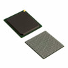
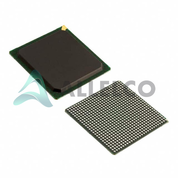
XC2V3000-4FGG676I (1)

Manufacturer Part Number

XC2V3000-4FGG676I

Manufacturer

Xilinx

Introduction

Virtex-II series FPGA for high-density, high-performance applications

Product Features and Performance

Integrated 3-million-gate FPGA

3584 Logic Cells/Configurable Logic Blocks

Total of 1,769,472 RAM bits for flexible on-chip storage

484 user-definable I/O pins

Support for a wide range of digital and mixed-signal applications

Product Advantages

Highly versatile for complex digital circuitry design

Ample I/O and memory resources to fit diverse needs

Robust surface mount design for secure PCB integration

Designed for low-power operation and heat management

Key Technical Parameters

3 million gates

3584 LABs/CLBs

1,769,472 Total RAM bits

484 I/O pins

425V to 1.575V supply voltage range

-40°C to 100°C operating temperature range

676-pin BGA package

Quality and Safety Features

Compliant with stringent industry standards

Built for rigorous industrial applications

Compatibility

Surface Mount technology

Compatible with 676-FBGA packaging systems

Application Areas

Data processing

Telecommunications

Industrial control systems

Networking

Digital signal processing

Product Lifecycle

Obsolete status

Check for potential replacement models or need for system upgrade

Several Key Reasons to Choose This Product

High gate count facilitates complex digital designs

Versatile in addressing various high-performance FPGA needs

Robust quality and safety standards cater to rigorous environments

Broad operating temperature suitable for diverse industrial applications

Support from Xilinx, a known leader in FPGA technologies

Frequently Asked Questions(FAQ)

What are the key power supply requirements and operating conditions for the XC2V3000-4FGG676I FPGA to ensure stable operation in industrial applications?
The XC2V3000-4FGG676I requires a tightly regulated core voltage between 1.425V and 1.575V, which is critical for maintaining signal integrity across its 484 I/O pins. This voltage tolerance reflects the device’s sensitivity to noise and transient fluctuations, particularly important in systems with multiple clock domains or high-speed serial transceivers. Operating within this window ensures proper logic switching margins and avoids setup/hold violations in synchronous designs. The specified junction temperature range of -40°C to 100°C supports deployment in harsh environments, but designers must account for thermal dissipation through adequate PCB layout and heatsinking, especially when utilizing the full complement of 3584 LABs and 1.77Mbit of block RAM.
How does the XC2V3000-4FGG676I compare to other Virtex-II FPGAs in terms of logic capacity and memory resources for mid-scale system-on-chip implementations?
With 3 million system gates, 3584 logic array blocks (LABs), and 1.77Mbit of distributed and block RAM combined, the XC2V3000-4FGG676I occupies a middle ground among Virtex-II family members. It offers significantly more logic density than smaller variants like the XC2V6000 but less than higher-end models such as the XC2VP30, making it suitable for complex state machines, moderate-width data paths, and embedded processor peripherals. Its balanced resource allocation supports designs requiring both control-plane logic and modest data buffering without overprovisioning, reducing BOM cost and board area compared to larger FPGAs.
What are the implications of using the XC2V3000-4FGG676I in high-reliability or safety-critical systems, given its historical release cycle and lifecycle status?
As a member of the Virtex-II generation, the XC2V3000-4FGG676I benefits from mature manufacturing processes and well-understood aging characteristics, which enhances long-term reliability in fixed-function applications. However, its discontinued evaluation status means that new design-ins should verify availability through authorized distributors and consider migration plans to modern families like Kintex UltraScale+ or Zynq-7000 if future scalability or security features are required. The device’s single-event upset (SEU) susceptibility remains consistent with SRAM-based FPGAs of its era, necessitating mitigation techniques such as scrubbing in mission-critical configurations.
How should the XC2V3000-4FGG676I be configured during startup to prevent configuration errors and ensure correct initialization in multi-device cascaded designs?
The XC2V3000-4FGG676I typically initiates configuration via SelectMAP or JTAG interfaces, depending on pin strapping at power-up. In master mode, it drives external flash memory with a bitstream generated by Xilinx tools targeting the Virtex-II architecture. Proper pull-up/pull-down resistor placement on configuration pins (such as PROG_B and INIT_B) is essential to avoid undefined states. When cascading multiple Virtex-II devices, each must be addressed individually via chip-select lines, and timing constraints must respect the slower propagation delays associated with older configuration protocols. Failure to adhere to these practices can result in partial or corrupted programming.
What are the typical routing congestion challenges when implementing large arithmetic units or wide memory interfaces using the XC2V3000-4FGG676I, and how can they be mitigated?
Despite its substantial gate count, the XC2V3000-4FGG676I shares die area constraints common to all FPGA generations, meaning that dense interconnect between LABs can lead to routing congestion—especially in datapaths exceeding 32 bits or when instantiating multiple block RAMs in parallel. Designers often encounter increased place-and-route times and degraded timing closure for paths crossing regional boundaries. Mitigation strategies include partitioning logic into hierarchical modules, limiting global clock skew through careful net planning, and avoiding excessive use of carry chains across CLB boundaries. Floorplanning in Vivado or ISE helps allocate critical regions early in the synthesis flow.
Can the XC2V3000-4FGG676I support dynamic partial reconfiguration, and what are the architectural limitations compared to newer FPGA families?
No, the XC2V3000-4FGG676I does not natively support dynamic partial reconfiguration due to its reliance on static SRAM cells and lack of dedicated reconfiguration controllers present in later architectures. Any functional change requires full device reprogramming, increasing latency and interrupting system operation. For applications demanding runtime adaptability—such as protocol switching or adaptive filtering—designers must either reserve sufficient logic resources for duplicated functionality or migrate to a device supporting partial reconfiguration, like those in the Spartan-6 or Artix-7 series.
What is the expected MTBF (mean time between failures) for the XC2V3000-4FGG676I under normal operating conditions, and how do environmental factors influence its reliability?
While exact MTBF figures depend on usage patterns and environmental stress, the XC2V3000-4FGG676I exhibits typical SRAM-based FPGA failure rates in the range of 1E9 to 1E10 FIT (failures in time) under nominal 1.5V operation and 85°C case temperature. Elevated ambient temperatures accelerate electromigration in bond wires and solder joints, while high humidity may compromise moisture-sensitive levels (this device has MSL 3). Derating power consumption and ensuring clean VCCO supplies further extends operational lifespan, particularly in telecom and industrial control systems where continuous uptime is essential.
How does the XC2V3000-4FGG676I handle ESD protection at the package level, and what precautions are necessary during PCB assembly and handling?
The XC2V3000-4FGG676I integrates basic ESD diodes at I/O pads rated for ±2kV HBM (Human Body Model), per JEDEC standards. However, these are not sufficient for direct exposure to static charges above ±4kV. During reflow soldering, peak temperatures must remain below 260°C for no more than 10 seconds to prevent internal delamination. Handling boards with anti-static wrist straps and storing unpackaged parts in conductive foam reduces risk. Additionally, input signals should be filtered with series resistors and TVS diodes if connected to unprotected external interfaces.
What are the trade-offs between using distributed RAM versus block RAM in the XC2V3000-4FGG676I for implementing FIFO buffers in high-throughput data acquisition systems?
Distributed RAM implemented via LUTs in the XC2V3000-4FGG676I consumes logic resources but offers faster access times and lower latency for small depths (<64 words), ideal for register files or shift registers. Block RAM, though occupying dedicated silicon area, provides deeper storage (up to 18Kb per block) with lower power and better utilization for large FIFO structures. For a 256-word FIFO, block RAM typically yields better area efficiency and predictable timing, whereas distributed RAM may fragment available LABs. Choice depends on depth, speed requirements, and overall resource budget.
How should decoupling capacitors be selected and placed around the XC2V3000-4FGG676I to minimize power supply noise and ensure stable operation during dynamic switching events?
A combination of 0.1µF ceramic capacitors rated for 6.3V or higher should be placed within 2mm of each VCCO pin, supplemented by bulk capacitance (e.g., 4.7µF tantalum or polymer) near the FBGA center to handle low-frequency transients. Given the device’s 484 I/Os and 1.5V core supply, simultaneous switching can induce millivolt-level dips. High-quality MLCCs with X5R or X7R dielectrics are preferred for their stability across temperature. Stitching vias under the FBGA reduce ground inductance, and power planes should be solid and uninterrupted beneath the package footprint.
Is the XC2V3000-4FGG676I compatible with third-party synthesis tools, and what licensing or constraint file considerations apply during implementation?
Officially, the XC2V3000-4FGG676I is supported only by Xilinx ISE Design Suite, which includes proprietary libraries and constraint formats (.ucf). Third-party tools may generate synthesizable RTL but often fail to interpret timing constraints accurately or map primitives correctly without vendor-specific attributes. Users must manually annotate black-box components or rely on open-source alternatives like SymbiFlow, though support is limited. Always validate post-place-and-route timing reports against Xilinx-provided reference implementations to ensure compliance.
What is the maximum sustainable data rate achievable across backplane or point-to-point links using the XC2V3000-4FGG676I’s high-performance I/O banks?
While the XC2V3000-4FGG676I lacks integrated transceivers capable of multi-gigabit speeds, its general-purpose I/O supports LVCMOS and LVTTL signaling up to 400 Mbps in optimized configurations. Achieving sustained throughput requires careful timing closure, controlled impedance traces, and minimal crosstalk. For higher rates, external PHYs or serializer/deserializer (SerDes) chips interfaced via parallel buses must be used, introducing latency and complexity. Thus, the device is better suited for control-intensive rather than high-bandwidth data transfer applications.
How does the XC2V3000-4FGG676I perform in radiation-hardened or space-rated applications, and what modifications are needed for reliable operation in such environments?
The XC2V3000-4FGG676I is not radiation-hardened and exhibits significant single-event upset (SEU) vulnerability due to its commercial-grade SRAM technology. In space or high-altitude aviation systems, cumulative dose effects and latch-up risks demand mitigation via error-correcting codes (ECC), triple modular redundancy (TMR), and periodic configuration scrubbing. Alternatively, designers should select a hardened counterpart such as the XQR2V3000 from Xilinx’s RadHard portfolio, which offers equivalent logic resources with radiation-tolerant process nodes.
What are the recommended termination schemes for clock distribution networks driven by the XC2V3000-4FGG676I to minimize jitter and skew in synchronous digital designs?
Clock outputs from the XC2V3000-4FGG676I should employ source-series termination (a series resistor close to the driver) when driving long traces or multiple loads. For global clocks routed through BUFG primitives, ensure fanout is limited to avoid excessive capacitive loading. Differential pairs benefit from matched-length routing and controlled impedance. Avoid stubs on clock trees, and use H-tree topologies sparingly due to resource constraints. Skew between related clocks (e.g., read/write clocks) must be kept under 100 ps to meet hold-time requirements in DDR-like interfaces.
How does the XC2V3000-4FGG676I support soft-core processors such as MicroBlaze or PicoBlaze, and what memory mapping strategies optimize performance?
The XC2V3000-4FGG676I efficiently hosts soft-core processors by allocating block RAMs as instruction/data caches or local memory. Mapping program code into fast-access BRAM reduces fetch latency compared to distributed RAM. Address decoding should align with BRAM granularity (typically 18Kb blocks) to minimize wasted cycles. Interrupt vectors and peripheral registers are best placed in contiguous address ranges accessible within one clock cycle. DMA engines built from custom IP cores can offload data movement, leveraging the FPGA’s parallelism while keeping CPU overhead low.
What are the legal and regulatory considerations when sourcing the XC2V3000-4FGG676I internationally, given its ECCN classification and export restrictions?
Classified under ECCN 3A991D, the XC2V3000-4FGG676I is subject to U.S. Export Administration Regulations (EAR). Exporting to certain countries may require license exceptions or full authorization depending on end-use and destination. Importers must comply with local HTSUS codes (e.g., 8542.39.0001 in the US) and ensure REACH compliance, though the component itself is unaffected. Always consult current trade regulations before procurement, especially for defense, aerospace, or cryptographic applications where dual-use concerns apply.
How should PCB layer stackup be designed to accommodate the XC2V3000-4FGG676I’s 676-pin FBGA footprint while maintaining signal integrity and manufacturability?
A minimum of six layers is recommended: two signal layers adjacent to solid power/ground planes to provide low-impedance returns for high-speed nets, plus inner power planes for core (1.5V) and I/O rails. Via-in-pad technology simplifies routing under the ball grid array, but microvias may increase fabrication cost. Impedance-controlled traces (50Ω single-ended) are critical for clocks and bidirectional data lines. Thermal vias under the package improve heat dissipation to outer layers, aiding junction temperature management during extended operation.
What diagnostic and debug capabilities are available during development with the XC2V3000-4FGG676I, and how effective are them for troubleshooting timing violations or functional bugs?
The XC2V3000-4FGG676I supports boundary-scan (JTAG) via IEEE 1149.1, enabling in-circuit testing and limited logic probing. Integrated ChipScope Pro cores allow real-time monitoring of internal signals, though insertion consumes LABs. Timing analysis relies on Xilinx’s static timing analyzer, which highlights paths violating setup/hold windows. Functional debugging is aided by assertion-based verification and simulation models. However, unlike modern devices with embedded logic analyzers, visibility into deep pipeline stages requires manual instrumentation, prolonging debug cycles.

Parts with Similar Specifications

The three parts on the right have similar specifications to AMD XC2V3000-4FGG676I

Product Attribute XC2V3000-4FGG676C XC2V3000-4FG676I XC2V3000-4FG676C XC2V3000-5BFG957I
Part Number XC2V3000-4FGG676C XC2V3000-4FG676I XC2V3000-4FG676C XC2V3000-5BFG957I
Manufacturer AMD AMD AMD AMD
Package - Tape & Reel (TR) Tube Tape & Reel (TR)
Number of I/O - - - -
Voltage - Supply - - - -
Mounting Type - Surface Mount Through Hole Surface Mount
Number of LABs/CLBs - - - -
Number of Gates - - - -
Series - - - -
Total RAM Bits - - - -
Operating Temperature - -40°C ~ 85°C 0°C ~ 70°C -40°C ~ 85°C
Package / Case - 196-LFBGA 16-DIP (0.300', 7.62mm) 64-VFQFN Exposed Pad
Base Product Number - DAC34H84 MAX500 ADS62P42
Supplier Device Package - 196-NFBGA (12x12) 16-PDIP 64-VQFN (9x9)

XC2V3000-4FGG676I Datasheet PDF

Download XC2V3000-4FGG676I pdf datasheets and AMD documentation for XC2V3000-4FGG676I - AMD.

Datasheets
Virtex-II Platform FPGAs.pdf
PCN Obsolescence/ EOL
Spartan, Virtex, XC17V00 24/Apr/2013.pdf
PCN Design/Specification
Stamped Lids 18/Apr/2016.pdf
Environmental Information
Xilinx REACH211 Cert.pdf

Customer Reviews

Evaluation: 10 Articles

  • Nath***rooks
    Jun 11, 2026

    Installed this power component in a converter board. Output remained stable under different load conditions and thermal performance was better than expected.

  • Dani***alkerTech
    Jun 1, 2026

    Product works, but setup took more effort than expected. Once configured the MCU ran reliably, although documentation support felt older compared with newer platforms. Fine for maintenance projects.

  • Yuki***aka88
    May 26, 2026

    信号通信プロジェクトでこのRS-485トランシーバーを使用しました。設置は簡単で、長距離ケーブルでも通信は安定していました。消費電力も、以前使用していたものより低くなっています。

  • Stev***aker
    May 20, 2026

    Solid diode for power rectification. Works well in switching circuits.

  • Bran***Lewis
    May 11, 2026

    Compact FPGA with good performance. Suitable for basic signal processing tasks.

  • Oliv***arris
    May 7, 2026

    Reliable I/O expander. Works well in embedded control applications.

  • Jess***Jones
    Apr 17, 2026

    It offers good value for the price, and the specifications match the description. I’ve been using it for two days with no issues, and I’ll definitely buy it again if I need it in the future.

  • Mich***Smith
    Apr 17, 2026

    Shipping was on time, the component pins are neatly aligned, and I tested 10 of them with a multimeter—all readings were within the specified range. Highly recommended.

  • Aman***arris
    Apr 3, 2026

    It was great—the entire process, from placing the order to receiving the package, went very smoothly. The components were consistent, the price was fair, and I had a very pleasant shopping experience.

  • Mike***nch
    Apr 3, 2026

    Better than expected! The resistance and capacitance readings were spot-on, and it passed the test on the first try. The service was reliable, and the packaging was thoughtful—I highly recommend it.

Write a Review

Your Email address will not be published.

Shipment

Delivery Time

In-stock items can be shipped within 24 hours. Some parts will be arranged for delivery within 1-2 days from the date all items arrive at our warehouse. And Allelco ships order once a day at about 17:00, except Sunday. Once the goods are shipped, the estimated delivery time depends on the shipping methods and Delivery destination. The table below shows are the logistic time for some common countries.

Delivery Cost

  1. Use your express account for shipment if you have one.
  2. Use our account for the shipment. Refer to the table below for the approximate charges.
(Different time frame / countries / package size has different price.)

Delivery Method

  1. Global Common Shipment by DHL / UPS / FedEx / TNT / EMS / SF we support.
  2. Others more shipping ways, please get in touch with your customer manager.

Common Countries Logistic Time Reference
Region Country Logistic Time(Day)
America United States 5
Brazil 7
Europe Germany 5
United Kingdom 4
Italy 5
Oceania Australia 6
New Zealand 5
Asia India 4
Japan 4
Middle East Israel 6
DHL & FedEx Shipment Charges Reference
Shipment charges(KG) Reference DHL(USD$)
0.00kg-1.00kg USD$30.00 - USD$60.00
1.00kg-2.00kg USD$40.00 - USD$80.00
2.00kg-3.00kg USD$50.00 - USD$100.00
Note:
The above table is for reference only. There may have some data bias for the uncontrollable factors.
Contact us if you have any questions.
  • QC (Quality Warranty)
  • Payment Support
  • Packaging
  • Certifications & Memberships

QC (Quality Warranty)

Allelco is committed to exceeding customer expectations through customer service excellence, order accuracy, and on-time delivery.
This is achieved through our commitment to the continual improvement of our processes, services, and products.


Strict quality inspection builds a solid foundation for electronic component quality.
  1. Visual inspection
  2. Performance testing and reliability verification
  3. Standardized full-process testing
  4. Precise control of every parameter
We eliminate defective components and ensure the stable operation of electronic devices through professional quality standards.

Payment Support

The payment method can be chosen from the methods shown below: Wire Transfer (T/T, Bank Transfer), Western Union, Credit card, PayPal.
  • HKBea
  • Paypal
  • MasterCard
  • Western-Union
  • VISA
Stable Delivery, Sincere Partnership — Your Faithful Supply Chain Partner
  • Efficient Supply Management
  • Cost-Saving Procurement
  • Fast Sourcing & Delivery
Contact us if you have any questions.

Packaging

Electrostatic Discharge Protection and Handling

All electrostatic-sensitive components are handled in accordance with electrostatic discharge control procedures. The products are hermetically sealed in anti-static safe packaging to prevent electrostatic damage. Appropriate labeling is also applied for identification and traceability. This ensures product integrity during storage, handling and transportation.


ESD

Certifications & Memberships

Third-party certified, strict quality control. Our certification
  • ISO 9001: 2015
  • ISO 13485: 2016
  • ISO 14001: 2015
  • ISO 28000: 2007
  • ISO 45001: 2018
  • GB/T 27922-2011
  • SMTA
  • IPC
  • ESD
  • PSMA
XC2V3000-4FGG676I Image

XC2V3000-4FGG676I

AMD
32D-XC2V3000-4FGG676I

Want a better price? Add to Cart and Submit RFQ now, we'll contact you immediately.

0 RFQ
Shopping cart (0 Items)
It is empty.
Compare List (0 Items)
It is empty.
Feedback

Your feedback matters! At Allelco, we value the user experience and strive to improve it constantly.
Please share your comments with us via our feedback form, and we'll respond promptly.
Thank you for choosing Allelco.

Subject
E-mail
Comments
Captcha
Drag or click to upload file
Upload File
types: .xls, .xlsx, .doc, .docx, .jpg, .png and .pdf.
Max file size: 10MB