View All

Please refer to the English Version as our Official Version.Return

Europe
France(Français) Germany(Deutsch) Italy(Italia) Russian(русский) Poland(polski) Czech(Čeština) Luxembourg(Lëtzebuergesch) Netherlands(Nederland) Iceland(íslenska) Hungarian(Magyarország) Spain(español) Portugal(Português) Turkey(Türk dili) Bulgaria(Български език) Ukraine(Україна) Greece(Ελλάδα) Israel(עִבְרִית) Sweden(Svenska) Finland(Svenska) Finland(Suomi) Romania(românesc) Moldova(românesc) Slovakia(Slovenská) Denmark(Dansk) Slovenia(Slovenija) Slovenia(Hrvatska) Croatia(Hrvatska) Serbia(Hrvatska) Montenegro(Hrvatska) Bosnia and Herzegovina(Hrvatska) Lithuania(lietuvių) Spain(Português) Switzerland(Deutsch) United Kingdom(English)
Asia/Pacific
Japan(日本語) Korea(한국의) Thailand(ภาษาไทย) Malaysia(Melayu) Singapore(Melayu) Vietnam(Tiếng Việt) Philippines(Pilipino)
Africa, India and Middle East
United Arab Emirates(العربية) Iran(فارسی) Tajikistan(فارسی) India(हिंदी) Madagascar(malaɡasʲ)
South America / Oceania
New Zealand(Maori) Brazil(Português) Angola(Português) Mozambique(Português)
North America
United States(English) Canada(English) Haiti(Ayiti) Mexico(español)
HomeProductsIntegrated Circuits (ICs)Embedded - FPGAs (Field Programmable Gate Array)XC2VP40-5FF1152I
XC2VP40-5FF1152I Image
Image may be representation.
See specifications for product details.
EXPRESS OPTION
Payment method

XC2VP40-5FF1152I - AMD

Manufacturer Part Number
XC2VP40-5FF1152I
Manufacturer
AMD Xilinx
Allelco Part Number
32D-XC2VP40-5FF1152I
Warranty
1 Year Allelco Warranty - Find out more
Stock Status:
16,590 pcs available, New & Original
Parts Description
IC FPGA 692 I/O 1152FCBGA
Package
1152-FCBGA (35x35)
Data sheet
XC2VP40-5FF1152.pdf

PCN Obsolescence/ EOL

Mult Dev EOL 6/Jan/2020.pdf

Environmental Information

Xilinx REACH211 Cert.pdf
RoHs Status
 
Our certification
In stock: 16590

Required fields are indicated by an asterisk (*)
Please send RFQ, we will respond immediately.

Quantity

Specifications

XC2VP40-5FF1152I Tech Specifications
AMD - XC2VP40-5FF1152I technical specifications, attributes, parameters and parts with similar specifications to AMD - XC2VP40-5FF1152I

Product Attribute Attribute Value
Manufacturer AMD Xilinx
Voltage - Supply 1.425V ~ 1.575V
Total RAM Bits 3538944
Supplier Device Package 1152-FCBGA (35x35)
Series Virtex®-II Pro
Package / Case 1152-BBGA, FCBGA
Package Tray
Product Attribute Attribute Value
Operating Temperature -40°C ~ 100°C (TJ)
Number of Logic Elements/Cells 43632
Number of LABs/CLBs 4848
Number of I/O 692
Mounting Type Surface Mount
Base Product Number XC2VP40

Environmental & Export Classifications

ATTRIBUTE DESCRIPTION
RoHs Status RoHS non-compliant
Moisture Sensitivity Level (MSL) 4 (72 Hours)
REACH Status REACH Unaffected
ECCN 3A001A7A
HTSUS 8542.39.0001

Parts Introduction

XC2VP40-5FF1152I Image
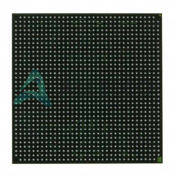
XC2VP40-5FF1152I (1)

Manufacturer Part Number

XC2VP40-5FF1152I

Manufacturer

Xilinx

Introduction

High-capacity, high-performance Virtex-II Pro FPGA with embedded IBM PowerPC processor blocks

Product Features and Performance

Embedded IBM PowerPC processor cores

4848 Logic Blocks/Configurable Logic Blocks (LABs/CLBs)

43632 Logic Elements/Cells

3538944 Total RAM Bits

Supports up to 692 I/O pins

FPGA integrated with multi-gigabit transceivers

Product Advantages

Integration of both logic and high-speed serial communication

High logic and memory resource count for complex applications

On-chip processor for embedded solutions

Robust temperature range for varied environmental conditions

Key Technical Parameters

Number of LABs/CLBs: 4848

Number of Logic Elements/Cells: 43632

Total RAM Bits: 3538944

Number of I/O: 692

Voltage Supply Range: 1.425V to 1.575V

Operating Temperature Range: -40°C to 100°C (TJ)

Quality and Safety Features

Surface Mount Technology for reliable solder connections

Extended operating temperature range for harsh environments

Compliant with industry quality standards for embedded applications

Compatibility

Compatible with various design suites for FPGA programming

Interoperable with other devices in the Virtex-II Pro series

Compatible with 1152-BBGA, FCBGA package specifications

Application Areas

Telecommunications

Aerospace and Defense Systems

Medical Equipment

High-Performance Computing Platforms

Industrial Automation Systems

Product Lifecycle

Obsolete status indicates discontinuation

Possible availability of replacement or upgrade options within the Xilinx product family

Several Key Reasons to Choose This Product

High integration of logic, memory, and processing capabilities reduces system complexity

Support for high-speed serial communication enables advanced data transfer capabilities

Wide operating temperature range suits various industrial and outdoor applications

Manufacturer with a strong reputation for quality and reliability in FPGA design

Potential for use in legacy systems requiring specific component specifications

Frequently Asked Questions(FAQ)

How does the XC2VP40-5FF1152I compare to other Virtex-II Pro FPGAs in terms of logic density and I/O count for high-speed data acquisition applications?
The XC2VP40-5FF1152I offers 43,632 logic elements and 692 I/O pins, providing significantly higher logic capacity than smaller variants like the XC2VP30, which supports up to 31,008 logic cells. This scalability makes the XC2VP40-5FF1152I suitable for complex digital signal processing and multi-channel data acquisition systems where routing congestion and timing closure are critical. The increased I/O count allows direct interfacing with multiple high-speed converters or memory interfaces without requiring external multiplexers.
What are the thermal considerations when deploying the XC2VP40-5FF1152I in industrial control systems operating near its maximum junction temperature?
With an operating range of -40°C to 100°C (TJ), the XC2VP40-5FF1152I can be used reliably in harsh environments, but sustained operation near 100°C demands careful thermal management. Given its power dissipation profile typical of 1.5 V FPGAs at full utilization, adequate heat sinking or airflow is essential to prevent thermal throttling or reduced mean time between failures. PCB layout should ensure thermal vias under the FCBGA package connect effectively to internal ground planes for heat spreading.
Can the XC2VP40-5FF1152I support DDR SDRAM interfaces directly, and what design challenges might arise due to its voltage domain and pin limitations?
While the XC2VP40-5FF1152I includes dedicated I/O banks capable of supporting LVDS and SSTL signaling, implementing DDR memory interfaces requires careful bank assignment due to strict voltage and reference requirements. Each bank operates within a tight 1.425V–1.575V supply window, incompatible with standard 1.8V or 2.5V DDR signals without level-shifters. Additionally, the 692 I/O limit may constrain memory channel count; designers must balance interface speed against available pins, often necessitating external buffers or switching to lower-pin-count alternatives.
How does the XC2VP40-5FF1152I’s MSL rating impact assembly reliability for long-life embedded systems compared to components with lower Moisture Sensitivity Levels?
Rated at MSL 4 (72 hours), the XC2VP40-5FF1152I requires stricter handling protocols during reflow soldering than MSL 1–3 parts. For mission-critical embedded systems with expected lifespans exceeding five years, uncontrolled storage humidity before assembly increases delamination risk at BGA joints. Manufacturers must enforce bake-out procedures and track shelf life rigorously—especially in humid climates—to avoid popcorning and latent reliability failures that could manifest years after deployment.
In what scenarios would the XC2VP40-5FF1152I be preferable over modern mid-range FPGAs despite its legacy status and RoHS non-compliance?
The XC2VP40-5FF1152I remains viable in legacy system upgrades or retrofit projects where board space, pin compatibility, or firmware reuse justifies continued use. Its deterministic architecture and proven timing models benefit safety-certified systems already qualified on this part. However, for new designs requiring regulatory compliance or long-term supply assurance, newer families like Kintex-7 offer better integration, lower static power, and RoHS compliance—making the XC2VP40-5FF1152I a niche choice rather than a forward-looking solution.
What trade-offs exist between using all 692 I/Os versus reserving pins for future expansion when selecting the XC2VP40-5FF1152I for a modular test instrumentation platform?
Allocating all 692 I/Os maximizes current functionality but reduces flexibility for later revisions. Given the fixed pinout of the 1152-FCBGA package, adding features post-manufacturing risks redesign costs. Engineers often reserve 10–15% of I/Os for debugging, calibration, or protocol updates. Alternatively, partitioning banks into dedicated function groups (e.g., one for sensors, another for comms) improves signal integrity and simplifies EMC validation—critical when scaling from prototype to production.
How does the XC2VP40-5FF1152I’s RAM block configuration affect real-time data buffering in video processing pipelines compared to simpler FPGA architectures?
With 3,538,944 total RAM bits organized into distributed and block RAM, the XC2VP40-5FF1152I supports deep line buffers for HD video streams without external memory. However, block RAM is non-uniformly distributed across CLBs, complicating memory mapping. Designers must manually partition pipelines to align with physical blocks, increasing synthesis complexity. This contrasts with modern FPGAs offering uniform BRAM distribution, reducing latency unpredictability in pixel stream processing.
Are there known yield or availability constraints associated with the XC2VP40-5FF1152I that could affect long-term production planning?
As a discontinued product with RoHS non-compliance status, the XC2VP40-5FF1152I faces sourcing volatility. Lead times may exceed 26 weeks during shortages, and end-of-life notifications from distributors signal declining inventory. For stable production runs beyond two years, engineers should evaluate migration paths to supported alternatives—even if performance margins are tighter—to mitigate supply chain disruption risks inherent in legacy semiconductor procurement.

Parts with Similar Specifications

The three parts on the right have similar specifications to AMD XC2VP40-5FF1152I

Product Attribute XC2VP40-5FFG1152I XC2VP40-5FF1152C XC2VP40-5FFG1152C XC2VP40-5FF1148I
Part Number XC2VP40-5FFG1152I XC2VP40-5FF1152C XC2VP40-5FFG1152C XC2VP40-5FF1148I
Manufacturer AMD AMD AMD AMD
Number of Logic Elements/Cells - - - -
Voltage - Supply - - - -
Total RAM Bits - - - -
Package / Case - 196-LFBGA 16-DIP (0.300', 7.62mm) 64-VFQFN Exposed Pad
Supplier Device Package - 196-NFBGA (12x12) 16-PDIP 64-VQFN (9x9)
Number of LABs/CLBs - - - -
Base Product Number - DAC34H84 MAX500 ADS62P42
Mounting Type - Surface Mount Through Hole Surface Mount
Operating Temperature - -40°C ~ 85°C 0°C ~ 70°C -40°C ~ 85°C
Series - - - -
Number of I/O - - - -
Package - Tape & Reel (TR) Tube Tape & Reel (TR)

XC2VP40-5FF1152I Datasheet PDF

Download XC2VP40-5FF1152I pdf datasheets and AMD documentation for XC2VP40-5FF1152I - AMD.

Datasheets
Virtex-II Pro, Pro X.pdf
PCN Obsolescence/ EOL
Mult Dev EOL 6/Jan/2020.pdf
Environmental Information
Xilinx REACH211 Cert.pdf

Customer Reviews

Evaluation: 10 Articles

  • Nath***rooks
    Jun 11, 2026

    Installed this power component in a converter board. Output remained stable under different load conditions and thermal performance was better than expected.

  • Dani***alkerTech
    Jun 1, 2026

    Product works, but setup took more effort than expected. Once configured the MCU ran reliably, although documentation support felt older compared with newer platforms. Fine for maintenance projects.

  • Yuki***aka88
    May 26, 2026

    信号通信プロジェクトでこのRS-485トランシーバーを使用しました。設置は簡単で、長距離ケーブルでも通信は安定していました。消費電力も、以前使用していたものより低くなっています。

  • Stev***aker
    May 20, 2026

    Solid diode for power rectification. Works well in switching circuits.

  • Bran***Lewis
    May 11, 2026

    Compact FPGA with good performance. Suitable for basic signal processing tasks.

  • Oliv***arris
    May 7, 2026

    Reliable I/O expander. Works well in embedded control applications.

  • Jess***Jones
    Apr 17, 2026

    It offers good value for the price, and the specifications match the description. I’ve been using it for two days with no issues, and I’ll definitely buy it again if I need it in the future.

  • Mich***Smith
    Apr 17, 2026

    Shipping was on time, the component pins are neatly aligned, and I tested 10 of them with a multimeter—all readings were within the specified range. Highly recommended.

  • Aman***arris
    Apr 3, 2026

    It was great—the entire process, from placing the order to receiving the package, went very smoothly. The components were consistent, the price was fair, and I had a very pleasant shopping experience.

  • Mike***nch
    Apr 3, 2026

    Better than expected! The resistance and capacitance readings were spot-on, and it passed the test on the first try. The service was reliable, and the packaging was thoughtful—I highly recommend it.

Write a Review

Your Email address will not be published.

Shipment

Delivery Time

In-stock items can be shipped within 24 hours. Some parts will be arranged for delivery within 1-2 days from the date all items arrive at our warehouse. And Allelco ships order once a day at about 17:00, except Sunday. Once the goods are shipped, the estimated delivery time depends on the shipping methods and Delivery destination. The table below shows are the logistic time for some common countries.

Delivery Cost

  1. Use your express account for shipment if you have one.
  2. Use our account for the shipment. Refer to the table below for the approximate charges.
(Different time frame / countries / package size has different price.)

Delivery Method

  1. Global Common Shipment by DHL / UPS / FedEx / TNT / EMS / SF we support.
  2. Others more shipping ways, please get in touch with your customer manager.

Common Countries Logistic Time Reference
Region Country Logistic Time(Day)
America United States 5
Brazil 7
Europe Germany 5
United Kingdom 4
Italy 5
Oceania Australia 6
New Zealand 5
Asia India 4
Japan 4
Middle East Israel 6
DHL & FedEx Shipment Charges Reference
Shipment charges(KG) Reference DHL(USD$)
0.00kg-1.00kg USD$30.00 - USD$60.00
1.00kg-2.00kg USD$40.00 - USD$80.00
2.00kg-3.00kg USD$50.00 - USD$100.00
Note:
The above table is for reference only. There may have some data bias for the uncontrollable factors.
Contact us if you have any questions.
  • QC (Quality Warranty)
  • Payment Support
  • Packaging
  • Certifications & Memberships

QC (Quality Warranty)

Allelco is committed to exceeding customer expectations through customer service excellence, order accuracy, and on-time delivery.
This is achieved through our commitment to the continual improvement of our processes, services, and products.


Strict quality inspection builds a solid foundation for electronic component quality.
  1. Visual inspection
  2. Performance testing and reliability verification
  3. Standardized full-process testing
  4. Precise control of every parameter
We eliminate defective components and ensure the stable operation of electronic devices through professional quality standards.

Payment Support

The payment method can be chosen from the methods shown below: Wire Transfer (T/T, Bank Transfer), Western Union, Credit card, PayPal.
  • HKBea
  • Paypal
  • MasterCard
  • Western-Union
  • VISA
Stable Delivery, Sincere Partnership — Your Faithful Supply Chain Partner
  • Efficient Supply Management
  • Cost-Saving Procurement
  • Fast Sourcing & Delivery
Contact us if you have any questions.

Packaging

Electrostatic Discharge Protection and Handling

All electrostatic-sensitive components are handled in accordance with electrostatic discharge control procedures. The products are hermetically sealed in anti-static safe packaging to prevent electrostatic damage. Appropriate labeling is also applied for identification and traceability. This ensures product integrity during storage, handling and transportation.


ESD

Certifications & Memberships

Third-party certified, strict quality control. Our certification
  • ISO 9001: 2015
  • ISO 13485: 2016
  • ISO 14001: 2015
  • ISO 28000: 2007
  • ISO 45001: 2018
  • GB/T 27922-2011
  • SMTA
  • IPC
  • ESD
  • PSMA
XC2VP40-5FF1152I Image

XC2VP40-5FF1152I

AMD
32D-XC2VP40-5FF1152I

Want a better price? Add to Cart and Submit RFQ now, we'll contact you immediately.

0 RFQ
Shopping cart (0 Items)
It is empty.
Compare List (0 Items)
It is empty.
Feedback

Your feedback matters! At Allelco, we value the user experience and strive to improve it constantly.
Please share your comments with us via our feedback form, and we'll respond promptly.
Thank you for choosing Allelco.

Subject
E-mail
Comments
Captcha
Drag or click to upload file
Upload File
types: .xls, .xlsx, .doc, .docx, .jpg, .png and .pdf.
Max file size: 10MB