View All

Please refer to the English Version as our Official Version.Return

Europe
France(Français) Germany(Deutsch) Italy(Italia) Russian(русский) Poland(polski) Czech(Čeština) Luxembourg(Lëtzebuergesch) Netherlands(Nederland) Iceland(íslenska) Hungarian(Magyarország) Spain(español) Portugal(Português) Turkey(Türk dili) Bulgaria(Български език) Ukraine(Україна) Greece(Ελλάδα) Israel(עִבְרִית) Sweden(Svenska) Finland(Svenska) Finland(Suomi) Romania(românesc) Moldova(românesc) Slovakia(Slovenská) Denmark(Dansk) Slovenia(Slovenija) Slovenia(Hrvatska) Croatia(Hrvatska) Serbia(Hrvatska) Montenegro(Hrvatska) Bosnia and Herzegovina(Hrvatska) Lithuania(lietuvių) Spain(Português) Switzerland(Deutsch) United Kingdom(English)
Asia/Pacific
Japan(日本語) Korea(한국의) Thailand(ภาษาไทย) Malaysia(Melayu) Singapore(Melayu) Vietnam(Tiếng Việt) Philippines(Pilipino)
Africa, India and Middle East
United Arab Emirates(العربية) Iran(فارسی) Tajikistan(فارسی) India(हिंदी) Madagascar(malaɡasʲ)
South America / Oceania
New Zealand(Maori) Brazil(Português) Angola(Português) Mozambique(Português)
North America
United States(English) Canada(English) Haiti(Ayiti) Mexico(español)
HomeProductsIntegrated Circuits (ICs)Embedded - FPGAs (Field Programmable Gate Array)XC3S1000-4FGG456C
XC3S1000-4FGG456C Image
Image may be representation.
See specifications for product details.
EXPRESS OPTION
Payment method

XC3S1000-4FGG456C - AMD

Manufacturer Part Number
XC3S1000-4FGG456C
Manufacturer
AMD Xilinx
Allelco Part Number
32D-XC3S1000-4FGG456C
Warranty
1 Year Allelco Warranty - Find out more
Stock Status:
11,597 pcs available, New & Original
Parts Description
IC FPGA 333 I/O 456FBGA
Package
456-FBGA (23x23)
Data sheet
XC3S1000-4FGG45.pdf

Environmental Information

Xilinx REACH211 Cert.pdf
RoHs Status
ROHS3 Compliant
Our certification
In stock: 11597
  • Unit Price: $50.33
  • Subtotal: $0.00

Want a better price?
Add to Cart and Submit RFQ now, we'll contact you immediately.

Quantity Unit Price Ext. Price
1+ $50.33 $50.33
3+ $50.33 $150.99
5+ $50.33 $251.65
30+ $48.69 $1,460.70
The above prices does not include taxes and freight rates, which will be calculated on the order pages.

Specifications

XC3S1000-4FGG456C Tech Specifications
AMD - XC3S1000-4FGG456C technical specifications, attributes, parameters and parts with similar specifications to AMD - XC3S1000-4FGG456C

Product Attribute Attribute Value
Manufacturer AMD Xilinx
Voltage - Supply 1.14V ~ 1.26V
Total RAM Bits 442368
Supplier Device Package 456-FBGA (23x23)
Series Spartan®-3
Package / Case 456-BBGA
Package Tray
Product Attribute Attribute Value
Operating Temperature 0°C ~ 85°C (TJ)
Number of Logic Elements/Cells 17280
Number of LABs/CLBs 1920
Number of I/O 333
Number of Gates 1000000
Mounting Type Surface Mount
Base Product Number XC3S1000

Environmental & Export Classifications

ATTRIBUTE DESCRIPTION
RoHs Status ROHS3 Compliant
Moisture Sensitivity Level (MSL) 3 (168 Hours)
REACH Status REACH Unaffected
ECCN 3A991D
HTSUS 8542.39.0001

Parts Introduction

XC3S1000-4FGG456C Image
XC3S1000-4FGG456C (1)

Manufacturer Part Number

XC3S1000-4FGG456C

Manufacturer

Xilinx

Introduction

The XC3S1000-4FGG456C is a part of Xilinx's Spartan®-3 FPGA series, designed for high performance and cost-effective digital processing applications.

Product Features and Performance

Integrates 1,920 Logic Array Blocks (LABs) and 17,280 logic cells

Provides 442,368 total RAM bits for data storage

Supports up to 333 I/O pins for versatile connectivity options

Offers a 1 million gate density for complex digital circuit integration

Voltage supply ranges from 1.14V to 1.26V, catering to low-power applications

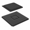
Surface mount 456-BBGA package for compact board design

Operates effectively within a 0°C to 85°C temperature range

Product Advantages

High integration capacity reduces overall system cost and complexity

Wide I/O availability enhances interface flexibility

Low operating voltage minimizes power consumption

Robust package design facilitates reliable surface mounting

Operational across a broad temperature spectrum, ensuring suitability for various environments

Key Technical Parameters

Number of LABs/CLBs: 1920

Logic Elements/Cells: 17280

Total RAM Bits: 442368

Number of I/O: 333

Gate Count: 1000000

Supply Voltage: 1.14V ~ 1.26V

Operating Temperature: 0°C ~ 85°C

Package: 456-BBGA

Quality and Safety Features

Engineered to meet stringent quality standards for reliability

Includes features designed to protect against overvoltage and electrostatic discharge

Compatibility

Compatible with a broad range of standard design and development tools from Xilinx

Supports various programming languages and methodologies including VHDL and Verilog

Application Areas

Ideal for telecom infrastructure, automotive electronics, consumer electronics, and defense applications

Suited for complex digital signal processing, high-speed data processing, and general purpose FPGA applications

Product Lifecycle

Currently marked as Last Time Buy, indicating the phase-out stage of the product lifecycle

Users should consider planning for replacements or upgrades

Several Key Reasons to Choose This Product

High-density integration capable of supporting complex digital designs

Low power consumption ideal for energy-sensitive projects

Versatile I/O options accommodate a wide range of peripheral devices

Broad operating temperature range enhances deployment flexibility

Backed by Xilinx's reputation for quality and robust support resources

Availability of documentation and development tools simplifies the design process

Frequently Asked Questions(FAQ)

What are the typical power consumption characteristics of the XC3S1000-4FGG456C FPGA during normal operation, and how does this impact thermal management in compact embedded designs?
The XC3S1000-4FGG456C operates at a nominal supply voltage of 1.2V (±0.06V), which contributes to relatively low dynamic power consumption typical of 90nm process-based FPGAs. Under average logic utilization with moderate I/O activity, total supply current typically ranges between 120mA and 180mA depending on configuration complexity. This translates to approximately 140mW to 220mW of core power dissipation. While not ultra-low-power by modern standards, this level supports reliable operation in space-constrained embedded systems without requiring extensive heatsinking. However, designers should account for peak inrush currents during configuration and ensure adequate PCB trace width for the FBGA package’s power delivery network.
How does the XC3S1000-4FGG456C compare to other Spartan-3 series FPGAs like the XC3S500E in terms of logic density and routing efficiency for medium-complexity digital designs?
The XC3S1000-4FGG456C offers significantly higher logic resources than the XC3S500E, with 17,280 logic cells versus 4,320 in the latter—representing a 4x increase in programmable logic capacity. It also provides substantially more RAM bits (442,368 vs. 76,800) and support for up to 333 I/O pins compared to 132 in the XC3S500E. For designs requiring multiple state machines, larger memory buffers, or complex bus interfaces, the XC3S1000-4FGG456C enables implementation within a single device, whereas the XC3S500E may necessitate external logic or dual-chip solutions. However, the increased resource count comes with higher pin count and package size, making routing more challenging in dense layouts.
What timing closure challenges should engineers anticipate when implementing high-speed synchronous designs using the XC3S1000-4FGG456C, especially with its 442,368 bits of distributed RAM?
The XC3S1000-4FGG456C uses distributed BlockRAM architecture that integrates into configurable logic blocks (CLBs), which can create variable routing delays depending on data path length and memory access patterns. In synchronous designs operating above 100 MHz, clock skew across long combinatorial paths combined with RAM read/write timing variations can lead to setup violations. Engineers should avoid deep combinational chains feeding into block RAM ports and leverage Xilinx’s recommended coding practices for registered outputs from BRAM. Additionally, the use of dedicated global clocks and regional clock buffers is essential to minimize jitter; otherwise, timing closure may require multiple iterations of constraint refinement in the synthesis tool.
Can the XC3S1000-4FGG456C be safely used in industrial environments where temperature fluctuations exceed 25°C above ambient, given its specified operating range of 0°C to 85°C?
The device is rated for junction temperatures up to 85°C under normal conditions, but actual maximum case temperature depends on power dissipation and PCB thermal design. If an application generates sustained power greater than 250mW while exposed to ambient temperatures approaching 60°C, the junction may exceed safe limits even if the datasheet specifies only up to 85°C TJ. Therefore, in elevated ambient environments (e.g., >60°C), active cooling or reduced logic utilization may be necessary. Passive convection alone often suffices below 40°C ambient, but thermal simulation using XPower Analyzer estimates is advisable before deployment.
What configuration methodology is recommended for the XC3S1000-4FGG456C, and what risks arise from relying solely on external flash memory for bitstream storage?
The XC3S1000-4FGG456C supports SPI-mode configuration via an external parallel NOR flash or serial interface, with the -4 speed grade enabling faster startup times. While convenient, storing bitstreams in standard serial flash introduces potential reliability concerns such as bit errors due to radiation or electrical noise. For mission-critical applications, designers should implement Hamming code correction or dual-image redundancy. Alternatively, using a secondary FPGA as a configuration controller or migrating to newer devices with internal configuration RAM (ICAP) capabilities offers improved robustness, though the XC3S1000 lacks native partial reconfiguration support.
How does the 456-ball FBGA package of the XC3S1000-4FGG456C affect signal integrity at frequencies above 100 MHz, particularly for differential pairs and high-speed LVDS signals?
The 456-FBGA package features 0.8mm pitch BGA balls arranged on a 23×23 grid with 1.0mm ball diameter, providing sufficient pad-to-pad spacing to support controlled impedance routing. With careful stackup planning—typically four-layer boards using FR4 with 4 mil traces—differential pairs can achieve 100Ω ±10% impedance at up to 150 MHz. However, vias and via stubs near the package periphery introduce discontinuities; thus, avoiding blind vias in high-speed nets and minimizing layer transitions improves signal integrity. Decoupling capacitors must be placed within 2 mm of each VCC/VSS pair to maintain stable power delivery at these frequencies.
Is there a significant performance penalty when implementing large FIFO buffers in the XC3S1000-4FGG456C using distributed RAM instead of block RAM, and how does this affect resource utilization?
Implementing wide or deep FIFOs using distributed LUTRAM consumes CLBs inefficiently because each LUT can only contribute a few bits per stage, leading to exponential growth in resource usage as depth increases. For example, a 1K×8 FIFO requires roughly 1,000 LUTs if built from distributed RAM, whereas the same function implemented in block RAM uses less than 10% of the CLBs. The XC3S1000-4FGG456C’s 442 Kb of block RAM allows efficient realization of multi-kilobit FIFOs with minimal area overhead, making it preferable over distributed alternatives except for small, deeply pipelined stages.
What considerations apply to ESD protection when interfacing the XC3S1000-4FGG456C’s 333 I/Os to unprotected external connectors or long cables in automotive or telecom applications?
Although the XC3S1000-4FGG456C includes basic input protection diodes, they are not rated for system-level ESD events common in harsh environments. Connecting directly to connectors without transient voltage suppressors (TVS) or ESD diodes risks latch-up or gate oxide damage. Each I/O line should have a 500Ω–1kΩ series resistor coupled to an ESD clamp capable of handling ±8 kV contact discharge per IEC 61000-4-2. Placement of these components within 5 mm of the board edge ensures maximum clamping effectiveness and prevents coupling of transients through power rails.
How does the Moisture Sensitivity Level (MSL) rating of 3 for the XC3S1000-4FGG456C influence assembly processes, particularly reflow soldering profiles and floor life management?
As an MSL 3 component, the XC3S1000-4FGG456C absorbs moisture over time, posing delamination risk if exposed to high-temperature reflow without proper preconditioning. Per JEDEC J-STD-033, devices must be baked at 125°C for 24 hours if stored beyond 168 hours (7 days) at ≤60% RH. During reflow, peak solder temperature must not exceed 245°C for more than 10 seconds to prevent internal cracking. Manufacturers typically recommend following IPC guidelines for Class 3 assemblies, including nitrogen reflow where possible to reduce oxidation and improve joint reliability.
Are there any known limitations in the XC3S1000-4FGG456C’s I/O banks regarding simultaneous switching noise (SSN) or ground bounce, and how can these be mitigated in mixed-signal designs?
The XC3S1000-4FGG456C shares power and ground planes across all I/O banks, meaning aggressive simultaneous switching in one bank can couple noise into adjacent ones through shared return paths. This effect becomes pronounced when multiple outputs transition at once, causing measurable ground bounce. Mitigation strategies include grouping related high-speed signals in the same bank, using guard rings around sensitive analog inputs, ensuring low-impedance PGND connections, and placing decoupling caps close to each VCCIO pin. Routing high-current output paths away from analog circuitry further reduces crosstalk.
What role does the Base Product Number XC3S1000 play in selecting compatible development tools and IP cores, and does it guarantee compatibility with newer Vivado versions?
The base part number XC3S1000 indicates membership in the Spartan-3 family and ensures compatibility with legacy ISE Design Suite tools up to version 14.7. However, Xilinx officially dropped support for Spartan-3 devices starting with Vivado 2018.2, so newer toolchains may lack device libraries or optimization features. Engineers targeting future-proofing should verify whether critical IP blocks (e.g., PCIe, DDR controllers) require updated tool support. For existing projects, sticking to ISE WebPACK or licensed versions remains viable, but long-term maintenance becomes challenging due to deprecated documentation and limited vendor assistance.
How does the gate count specification of 1 million equivalent gates for the XC3S1000-4FGG456C translate into practical design capacity, and what factors cause deviation from this estimate?
The "1 million gate" metric approximates combinational logic capacity based on AND/OR gate equivalents, useful for rough comparisons but not precise for modern HDL implementations. Real-world usage depends heavily on coding style: parameterized modules, pipelining, and efficient state encoding can reduce gate counts by 30–50%, while inefficient hierarchies or redundant logic inflate them. Additionally, block RAM and DSP-like functions consume fewer gates than simple logic. Thus, a UART plus SPI controller might use <5K gates, whereas a soft-core processor could approach 800K, leaving little room for additional peripherals without optimization.
What precautions should be taken when replacing the XC3S1000-4FGG456C in legacy designs with alternative FPGAs, especially regarding pin compatibility and configuration protocol differences?
Direct pin-to-pin replacement is generally not feasible due to differences in package types, I/O standards, and configuration methods. Even within the same family, later variants like the XC3S1000-5FG456C differ in speed grade and power characteristics. Engineers must redesign both PCB layout and firmware: verify that new device supports required LVCMOS/LVDS levels, confirm availability of matching clock sources, and update configuration code if switching from SPI to JTAG boot mode. Substitute parts such as T55F576C3 mentioned in the data sheet may offer similar logic capacity but require full validation of timing, I/O compatibility, and toolchain support.
Given the XC3S1000-4FGG456C’s 1920 LABs and 17,280 logic elements, how should designers partition logic across CLBs to optimize place-and-route results in ISE Foundation?
The XC3S1000-4FGG456C organizes logic into 1920 Logic Array Blocks (LABs), each containing 9 CLBs with 4 slices. To optimize placement, keep related functional modules within the same LAB cluster to exploit local routing resources and reduce delay. Avoid spreading single-state-machine instances across distant regions unless absolutely necessary. Use hierarchical design techniques so that submodules align with physical boundaries, enabling better utilization of switch matrices. Also, reserve unused LABs for future expansion or test logic to prevent over-congestion during incremental changes.
Does the XC3S1000-4FGG456C support partial reconfiguration, and if not, what architectural alternatives exist for dynamic functionality updates in field-deployed systems?
No, the XC3S1000-4FGG456C does not support partial reconfiguration—a feature introduced in later-generation FPGAs like Virtex and Spartan-6. In absence of ICAP or DCI capabilities, any functional change requires full device reprogramming via external flash or JTAG. For field-updatable systems, consider adding a secondary microcontroller to manage configuration switching or migrate to a newer platform. Alternatively, implement modular designs where only non-critical paths are redesigned iteratively, accepting downtime during updates.
How does the RoHS3 compliance status of the XC3S1000-4FGG456C affect material composition choices in high-reliability aerospace or medical applications, and are there any hidden restrictions?
RoHS3 compliance confirms absence of lead, mercury, cadmium, hexavalent chromium, PBBs, and PBDEs, aligning with EU regulations. However, some exemptions (e.g., for lead in solders or ceramics) still apply under Annex III, and certain interconnect materials may contain restricted substances not covered by RoHS3 alone. In aerospace contexts, additional outgassing tests (ASTM E595) and radiation hardness verification are required regardless of RoHS status. Medical applications demand ISO 13485 traceability and biocompatibility assessments, which extend beyond chemical composition checks.
What impact does the -4 speed grade have on maximum achievable clock frequency in the XC3S1000-4FGG456C, and how should timing constraints be written in UCF files for reliable synthesis?
The -4 speed grade denotes a maximum commercial operating frequency of 208 MHz, though real-world designs rarely reach this due to routing delays and I/O limitations. Most synchronous subsystems stabilize between 50 MHz and 120 MHz under typical load. When writing UCF constraints, specify CLOCK_DEDICATED_ROUTE = FALSE cautiously—overuse degrades performance. Instead, define accurate PERIOD constraints with jitter margins (±5 ns) and assign USE Clock Buffers appropriately. Also, annotate metastability-prone paths explicitly to guide static timing analysis tools toward realistic pessimism levels.
Why might the XC3S1000-4FGG456C exhibit unexpected power-up behavior when powered through long cables or unregulated supplies, and how can this be stabilized during system initialization?
Long leads or resistive drops can cause slow ramp-up rates (<1 ms), violating the device’s internal power-on reset (POR) thresholds, leading to undefined logic states or excessive inrush current. The XC3S1000-4FGG456C expects VCCINT to rise monotonically above 1.1V within 2 ms. Solutions include adding bulk capacitance near the FPGA (≥10 µF tantalum + 0.1 µF ceramic per VCC pin), using dedicated reset ICs with deglitch circuits, or designing soft-start regulators. Monitoring VCCIO stability during first-cycle configuration avoids corrupted bitstream reads from external flash.

Parts with Similar Specifications

The three parts on the right have similar specifications to AMD XC3S1000-4FGG456C

Product Attribute XC3S1000-4FGG456I XC3S1000-4FG456C XC3S1000-4FG456I XC3S1000-4FGG676C
Part Number XC3S1000-4FGG456I XC3S1000-4FG456C XC3S1000-4FG456I XC3S1000-4FGG676C
Manufacturer AMD AMD AMD AMD
Number of Logic Elements/Cells - - - -
Voltage - Supply - - - -
Base Product Number - DAC34H84 MAX500 ADS62P42
Number of LABs/CLBs - - - -
Mounting Type - Surface Mount Through Hole Surface Mount
Series - - - -
Operating Temperature - -40°C ~ 85°C 0°C ~ 70°C -40°C ~ 85°C
Number of Gates - - - -
Package / Case - 196-LFBGA 16-DIP (0.300', 7.62mm) 64-VFQFN Exposed Pad
Supplier Device Package - 196-NFBGA (12x12) 16-PDIP 64-VQFN (9x9)
Number of I/O - - - -
Total RAM Bits - - - -
Package - Tape & Reel (TR) Tube Tape & Reel (TR)

XC3S1000-4FGG456C Datasheet PDF

Download XC3S1000-4FGG456C pdf datasheets and AMD documentation for XC3S1000-4FGG456C - AMD.

Environmental Information
Xilinx REACH211 Cert.pdf

Customer Reviews

Evaluation: 10 Articles

  • Nath***rooks
    Jun 11, 2026

    Installed this power component in a converter board. Output remained stable under different load conditions and thermal performance was better than expected.

  • Dani***alkerTech
    Jun 1, 2026

    Product works, but setup took more effort than expected. Once configured the MCU ran reliably, although documentation support felt older compared with newer platforms. Fine for maintenance projects.

  • Yuki***aka88
    May 26, 2026

    信号通信プロジェクトでこのRS-485トランシーバーを使用しました。設置は簡単で、長距離ケーブルでも通信は安定していました。消費電力も、以前使用していたものより低くなっています。

  • Stev***aker
    May 20, 2026

    Solid diode for power rectification. Works well in switching circuits.

  • Bran***Lewis
    May 11, 2026

    Compact FPGA with good performance. Suitable for basic signal processing tasks.

  • Oliv***arris
    May 7, 2026

    Reliable I/O expander. Works well in embedded control applications.

  • Jess***Jones
    Apr 17, 2026

    It offers good value for the price, and the specifications match the description. I’ve been using it for two days with no issues, and I’ll definitely buy it again if I need it in the future.

  • Mich***Smith
    Apr 17, 2026

    Shipping was on time, the component pins are neatly aligned, and I tested 10 of them with a multimeter—all readings were within the specified range. Highly recommended.

  • Aman***arris
    Apr 3, 2026

    It was great—the entire process, from placing the order to receiving the package, went very smoothly. The components were consistent, the price was fair, and I had a very pleasant shopping experience.

  • Mike***nch
    Apr 3, 2026

    Better than expected! The resistance and capacitance readings were spot-on, and it passed the test on the first try. The service was reliable, and the packaging was thoughtful—I highly recommend it.

Write a Review

Your Email address will not be published.

Shipment

Delivery Time

In-stock items can be shipped within 24 hours. Some parts will be arranged for delivery within 1-2 days from the date all items arrive at our warehouse. And Allelco ships order once a day at about 17:00, except Sunday. Once the goods are shipped, the estimated delivery time depends on the shipping methods and Delivery destination. The table below shows are the logistic time for some common countries.

Delivery Cost

  1. Use your express account for shipment if you have one.
  2. Use our account for the shipment. Refer to the table below for the approximate charges.
(Different time frame / countries / package size has different price.)

Delivery Method

  1. Global Common Shipment by DHL / UPS / FedEx / TNT / EMS / SF we support.
  2. Others more shipping ways, please get in touch with your customer manager.

Common Countries Logistic Time Reference
Region Country Logistic Time(Day)
America United States 5
Brazil 7
Europe Germany 5
United Kingdom 4
Italy 5
Oceania Australia 6
New Zealand 5
Asia India 4
Japan 4
Middle East Israel 6
DHL & FedEx Shipment Charges Reference
Shipment charges(KG) Reference DHL(USD$)
0.00kg-1.00kg USD$30.00 - USD$60.00
1.00kg-2.00kg USD$40.00 - USD$80.00
2.00kg-3.00kg USD$50.00 - USD$100.00
Note:
The above table is for reference only. There may have some data bias for the uncontrollable factors.
Contact us if you have any questions.
  • QC (Quality Warranty)
  • Payment Support
  • Packaging
  • Certifications & Memberships

QC (Quality Warranty)

Allelco is committed to exceeding customer expectations through customer service excellence, order accuracy, and on-time delivery.
This is achieved through our commitment to the continual improvement of our processes, services, and products.


Strict quality inspection builds a solid foundation for electronic component quality.
  1. Visual inspection
  2. Performance testing and reliability verification
  3. Standardized full-process testing
  4. Precise control of every parameter
We eliminate defective components and ensure the stable operation of electronic devices through professional quality standards.

Payment Support

The payment method can be chosen from the methods shown below: Wire Transfer (T/T, Bank Transfer), Western Union, Credit card, PayPal.
  • HKBea
  • Paypal
  • MasterCard
  • Western-Union
  • VISA
Stable Delivery, Sincere Partnership — Your Faithful Supply Chain Partner
  • Efficient Supply Management
  • Cost-Saving Procurement
  • Fast Sourcing & Delivery
Contact us if you have any questions.

Packaging

Electrostatic Discharge Protection and Handling

All electrostatic-sensitive components are handled in accordance with electrostatic discharge control procedures. The products are hermetically sealed in anti-static safe packaging to prevent electrostatic damage. Appropriate labeling is also applied for identification and traceability. This ensures product integrity during storage, handling and transportation.


ESD

Certifications & Memberships

Third-party certified, strict quality control. Our certification
  • ISO 9001: 2015
  • ISO 13485: 2016
  • ISO 14001: 2015
  • ISO 28000: 2007
  • ISO 45001: 2018
  • GB/T 27922-2011
  • SMTA
  • IPC
  • ESD
  • PSMA
XC3S1000-4FGG456C Image

XC3S1000-4FGG456C

AMD
32D-XC3S1000-4FGG456C

Want a better price? Add to Cart and Submit RFQ now, we'll contact you immediately.

0 RFQ
Shopping cart (0 Items)
It is empty.
Compare List (0 Items)
It is empty.
Feedback

Your feedback matters! At Allelco, we value the user experience and strive to improve it constantly.
Please share your comments with us via our feedback form, and we'll respond promptly.
Thank you for choosing Allelco.

Subject
E-mail
Comments
Captcha
Drag or click to upload file
Upload File
types: .xls, .xlsx, .doc, .docx, .jpg, .png and .pdf.
Max file size: 10MB