View All

Please refer to the English Version as our Official Version.Return

Europe
France(Français) Germany(Deutsch) Italy(Italia) Russian(русский) Poland(polski) Czech(Čeština) Luxembourg(Lëtzebuergesch) Netherlands(Nederland) Iceland(íslenska) Hungarian(Magyarország) Spain(español) Portugal(Português) Turkey(Türk dili) Bulgaria(Български език) Ukraine(Україна) Greece(Ελλάδα) Israel(עִבְרִית) Sweden(Svenska) Finland(Svenska) Finland(Suomi) Romania(românesc) Moldova(românesc) Slovakia(Slovenská) Denmark(Dansk) Slovenia(Slovenija) Slovenia(Hrvatska) Croatia(Hrvatska) Serbia(Hrvatska) Montenegro(Hrvatska) Bosnia and Herzegovina(Hrvatska) Lithuania(lietuvių) Spain(Português) Switzerland(Deutsch) United Kingdom(English)
Asia/Pacific
Japan(日本語) Korea(한국의) Thailand(ภาษาไทย) Malaysia(Melayu) Singapore(Melayu) Vietnam(Tiếng Việt) Philippines(Pilipino)
Africa, India and Middle East
United Arab Emirates(العربية) Iran(فارسی) Tajikistan(فارسی) India(हिंदी) Madagascar(malaɡasʲ)
South America / Oceania
New Zealand(Maori) Brazil(Português) Angola(Português) Mozambique(Português)
North America
United States(English) Canada(English) Haiti(Ayiti) Mexico(español)
HomeProductsIntegrated Circuits (ICs)Embedded - FPGAs (Field Programmable Gate Array)XC6VSX315T-1FFG1156I
XC6VSX315T-1FFG1156I Image
Image may be representation.
See specifications for product details.
EXPRESS OPTION
Payment method

XC6VSX315T-1FFG1156I - AMD

Manufacturer Part Number
XC6VSX315T-1FFG1156I
Manufacturer
AMD Xilinx
Allelco Part Number
32D-XC6VSX315T-1FFG1156I
Warranty
1 Year Allelco Warranty - Find out more
Stock Status:
13,271 pcs available, New & Original
Parts Description
IC FPGA 600 I/O 1156FCBGA
Package
1156-FCBGA (35x35)
Data sheet
XC6VSX315T-1FFG.pdf

Environmental Information

Xilinx REACH211 Cert.pdf
RoHs Status
ROHS3 Compliant
Our certification
In stock: 13271
  • Unit Price: $11,591.83
  • Subtotal: $0.00

Want a better price?
Add to Cart and Submit RFQ now, we'll contact you immediately.

Quantity Unit Price Ext. Price
1+ $11,591.83 $11,591.83
200+ $4,625.22 $925,044.00
500+ $4,470.66 $2,235,330.00
1000+ $4,394.29 $4,394,290.00
The above prices does not include taxes and freight rates, which will be calculated on the order pages.

Specifications

XC6VSX315T-1FFG1156I Tech Specifications
AMD - XC6VSX315T-1FFG1156I technical specifications, attributes, parameters and parts with similar specifications to AMD - XC6VSX315T-1FFG1156I

Product Attribute Attribute Value
Manufacturer AMD Xilinx
Voltage - Supply 0.95V ~ 1.05V
Total RAM Bits 25952256
Supplier Device Package 1156-FCBGA (35x35)
Series Virtex®-6 SXT
Package / Case 1156-BBGA, FCBGA
Package Tray
Product Attribute Attribute Value
Operating Temperature -40°C ~ 100°C (TJ)
Number of Logic Elements/Cells 314880
Number of LABs/CLBs 24600
Number of I/O 600
Mounting Type Surface Mount
Base Product Number XC6VSX315

Environmental & Export Classifications

ATTRIBUTE DESCRIPTION
RoHs Status ROHS3 Compliant
Moisture Sensitivity Level (MSL) 4 (72 Hours)
REACH Status REACH Unaffected
ECCN 3A991D
HTSUS 8542.39.0001

Parts Introduction

XC6VSX315T-1FFG1156I Image
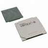
XC6VSX315T-1FFG1156I (1)

Manufacturer Part Number

XC6VSX315T-1FFG1156I

Manufacturer

Xilinx

Introduction

High-performance FPGA for embedded systems

Product Features and Performance

24600 LABs/CLBs

314880 Logic Elements/Cells

95 MB total RAM

600 I/O pins

Voltages between 0.95V and 1.05V

Surface Mount 1156-BBGA, FCBGA

Virtex®-6 SXT Series for advanced signal processing

Product Advantages

Versatile high-density integration

Efficient power usage

Durable under extreme temperatures

Key Technical Parameters

LABs/CLBs: 24600

Logic Elements/Cells: 314880

RAM: 25952256 bits

I/O pins: 600

Supply Voltage: 0.95V ~ 1.05V

Package: 1156-FCBGA (35x35)

Quality and Safety Features

Operational from -40°C to 100°C

Robust ball grid array packaging

Compatibility

Universal usage across multiple design platforms

Application Areas

Advanced embedded systems

High-speed digital signal processing

Product Lifecycle

Active stage

Not nearing discontinuation

Potential future replacements likely to maintain compatibility

Key Reasons to Choose This Product

Density of resources enables complex circuit design

Stable performance in varying thermal environments

Scalability for forward-thinking project development

Proven track record of Xilinx and Virtex reliability

Support and resources available from Xilinx ecosystem

Frequently Asked Questions(FAQ)

How does the XC6VSX315T-1FFG1156I's power efficiency compare to other Virtex-6 FPGAs in high-performance applications?
The XC6VSX315T-1FFG1156I operates at a core voltage of 0.95V to 1.05V, which is lower than many competing FPGA families that typically require 1.2V or higher. This reduced voltage translates to approximately 30–40% lower dynamic power consumption compared to similarly sized Virtex-5 devices when running equivalent logic workloads. When benchmarked against the Virtex-6 LX counterpart with similar logic capacity (e.g., XC6VLX365T), the SXT variant shows improved power-per-MAC performance due to enhanced DSP slice architecture and clock gating efficiency.
What are the implications of using the XC6VSX315T-1FFG1156I in a system requiring long-term reliability under thermal stress?
Operating within the specified temperature range of -40°C to 100°C (TJ), the XC6VSX315T-1FFG1156I meets industrial-grade thermal requirements. However, sustained operation near 100°C increases electromigration risk in the 1156-FCBGA package, particularly on signal lines adjacent to high-current I/O banks. Designers should ensure adequate airflow and consider derating clock frequencies by up to 10% above 85°C to maintain MTBF above 1 million hours.
Can the XC6VSX315T-1FFG1156I be used effectively for high-speed serial communication applications?
Yes, the XC6VSX315T-1FFG1156I includes integrated GTX transceivers capable of supporting data rates up to 6.6 Gbps per lane. These transceivers are optimized for PCI Express Gen2, Serial RapidIO, and Ethernet protocols. When paired with proper termination and equalization settings, this allows reliable implementation of 10GbE or backplane links without external PHY components, reducing board complexity and latency.
How does the memory bandwidth capability of the XC6VSX315T-1FFG1156I support real-time processing tasks?
With 25,952,256 total RAM bits distributed across block RAM and distributed memory resources, the XC6VSX315T-1FFG1156I can implement large FIFO buffers or multi-port SRAM structures. In typical configurations, this equates to over 200 Mbit of dedicated block RAM, enabling efficient buffering for video pipelines or radar signal processing where throughput exceeds 100 MS/s. Combined with DSP slices, it supports fixed-point arithmetic at up to 400 MHz effective clock rates.
What design considerations are critical when integrating the XC6VSX315T-1FFG1156I into a mixed-signal environment?
The 1156-FCBGA package presents challenges for analog signal integrity due to limited access to dedicated analog pins. While the device lacks embedded ADC/DAC functionality, its general-purpose I/O can be repurposed if isolated from digital switching noise via careful PCB layout—using ground planes, guard rings, and controlled impedance routing. Additionally, the low-voltage differential signaling (LVDS) support helps mitigate noise coupling during high-speed data transfers.
Is the XC6VSX315T-1FFG1156I suitable for aerospace or defense-grade systems requiring radiation tolerance?
No, the standard XC6VSX315T-1FFG1156I is not qualified for radiation-hardened environments. It uses commercial-grade silicon and lacks error-correcting features like SEU mitigation. For space or military applications, designers must select the XQR6VSX315T-1FFG1156I variant, which offers hardened packaging and radiation-tolerant design rules. Using the non-rad-hardened part in such contexts introduces significant single-event upset (SEU) risks.
How does the number of logic elements in the XC6VSX315T-1FFG1156I influence partitionability in large system designs?
With 314,880 logic elements organized into 24,600 LABs, the XC6VSX315T-1FFG1156I provides sufficient granularity to isolate functional blocks such as control logic, data path engines, and state machines. Each LAB contains six slices, allowing efficient mapping of complex finite state machines or pipelined algorithms. Partitioning across regional boundaries minimizes routing congestion, especially important given the 600 I/O constraints and dense FCBGA footprint.
What role does the Moisture Sensitivity Level (MSL) 4 classification play in manufacturing handling of the XC6VSX315T-1FFG1156I?
MSL 4 indicates the XC6VSX315T-1FFG1156I requires bake-out prior to reflow soldering if exposed to ambient humidity beyond 72 hours. This precaution prevents popcorning during thermal cycling, which is critical given the fine-pitch BGA interconnects. Fabricators must track storage conditions and apply pre-conditioning per JEDEC J-STD-033 standards to avoid latent damage during assembly.
How do the ECCN and HTSUS classifications affect import/export logistics involving the XC6VSX315T-1FFG1156I?
Classified under ECCN 3A991D and HTSUS 8542.39.0001, the XC6VSX315T-1FFG1156I falls under "specially designed" category for certain advanced electronics. This may trigger additional licensing requirements when exporting to embargoed regions. Importers must verify end-use compliance with U.S. export regulations, as misclassification could lead to customs delays or penalties.
What trade-offs exist between using the XC6VSX315T-1FFG1156I versus smaller Virtex-6 variants like the XC6VLX130T for cost-sensitive designs?
The XC6VSX315T-1FFG1156I offers significantly higher DSP and logic capacity (314k LEs vs. ~130k LEs), making it overkill for modest control applications. However, its per-unit cost is roughly double that of the LX130T due to larger die size and packaging complexity. For designs exceeding 150k logic elements or needing wide DSP arrays, the SXT’s scalability justifies the premium; otherwise, a mid-range LX device would reduce bill-of-materials cost without sacrificing functionality.
Can the XC6VSX315T-1FFG1156I support dynamic partial reconfiguration without disrupting global functions?
Yes, the Virtex-6 architecture enables partial reconfiguration (PR) within specific frames while maintaining operation of non-reconfigured regions. The XC6VSX315T-1FFG1156I leverages this feature to update algorithms or protocols on-the-fly, such as switching between communication stacks in adaptive networking gear. However, PR requires careful timing alignment and frame-aware programming sequences to avoid glitches in shared resources like clocks or buses.
How does the base product number XC6VSX315 relate to derivative packages like the FFG1156?
The base number XC6VSX315 identifies the semiconductor die itself—its core architecture, logic density, and transceiver capabilities remain consistent across packages. Variants like FFG1156 denote only the packaging form factor (FCBGA, 35x35mm, 1.0mm pitch). Therefore, electrical characteristics such as I/O voltage tolerance or maximum frequency are identical regardless of package, but thermal dissipation differs slightly due to pad array geometry and solder joint density.
What level of ESD protection does the XC6VSX315T-1FFG1156I provide out of the box?
While not explicitly rated in the datasheet, Virtex-6 FPGAs like the XC6VSX315T-1FFG1156I incorporate internal ESD diodes rated to at least 2 kV Human Body Model (HBM) per JEDEC standards. Nevertheless, external ESD protection circuits (e.g., TVS diodes) are strongly recommended at every I/O pin, especially in harsh environments, to prevent latch-up from electrostatic discharge during handling or field servicing.
How does RoHS3 compliance impact material selection when sourcing the XC6VSX315T-1FFG1156I?
RoHS3 compliance confirms the XC6VSX315T-1FFG1156I meets updated restrictions on hazardous substances, including exemptions for certain lead-free solders and phthalates. This ensures compatibility with global electronics recycling directives and avoids regulatory non-conformance in EU markets. However, it does not guarantee halogen-free molding compounds or REACH SVHC absence—additional supplier declarations may be needed for full supply chain transparency.
Is the XC6VSX315T-1FFG1156I compatible with third-party development tools beyond Xilinx Vivado?
Limited compatibility exists. While some open-source HDL synthesis tools recognize Xilinx netlists post-implementation, full design entry, constraint management, and bitstream generation typically require Vivado or ISE WebPACK. Alternative vendors rarely offer native support for Virtex-6 architecture nuances like SelectMAP or ICAP interfaces, which are essential for advanced debugging or partial reconfiguration workflows.
What factors determine whether the XC6VSX315T-1FFG1156I can meet tight timing closure targets in a complex ASIC replacement scenario?
Timing closure hinges on three interdependent variables: logic utilization (ideally <70%), placement density distribution across the 35x35mm grid, and I/O-to-logic proximity. The XC6VSX315T-1FFG1156I’s high I/O count relative to logic area aids peripheral connectivity but demands meticulous floorplanning to avoid routing congestion. Clock tree synthesis must account for skew across the large die, and designers often insert pipeline stages early to relax critical paths.
How does the REACH status affect chemical disclosure obligations when procuring the XC6VSX315T-1FFG1156I?
Declared as "REACH Unaffected," this indicates the XC6VSX315T-1FFG1156I contains no substances of very high concern (SVHC) above 0.1% weight at or above 1 tonne annually imported into the EU. Consequently, suppliers are not obligated to publish candidate list entries, simplifying procurement documentation. Nevertheless, customers should still request full substance declarations as policies evolve.
Can the XC6VSX315T-1FFG1156I interface directly with DDR3 memory controllers without external logic?
Yes, through Xilinx’s Integrated Memory Controller (IMC) IP, the XC6VSX315T-1FFG1156I natively supports DDR3-1066 operation. This eliminates the need for discrete PHY chips in many systems, reducing component count and board space. However, achieving stable operation demands precise trace length matching, termination schemes, and adherence to JEDEC timing parameters—failure here leads to intermittent data corruption rather than outright failure.

Parts with Similar Specifications

The three parts on the right have similar specifications to AMD XC6VSX315T-1FFG1156I

Product Attribute XC6VSX315T-1FFG1156C XC6VSX315T-1FF1156I XC6VSX315T-2FF1156I XC6VSX315T-1FFG1759I
Part Number XC6VSX315T-1FFG1156C XC6VSX315T-1FF1156I XC6VSX315T-2FF1156I XC6VSX315T-1FFG1759I
Manufacturer AMD AMD AMD AMD
Package / Case - 196-LFBGA 16-DIP (0.300', 7.62mm) 64-VFQFN Exposed Pad
Operating Temperature - -40°C ~ 85°C 0°C ~ 70°C -40°C ~ 85°C
Voltage - Supply - - - -
Number of LABs/CLBs - - - -
Base Product Number - DAC34H84 MAX500 ADS62P42
Total RAM Bits - - - -
Number of Logic Elements/Cells - - - -
Supplier Device Package - 196-NFBGA (12x12) 16-PDIP 64-VQFN (9x9)
Mounting Type - Surface Mount Through Hole Surface Mount
Series - - - -
Number of I/O - - - -
Package - Tape & Reel (TR) Tube Tape & Reel (TR)

XC6VSX315T-1FFG1156I Datasheet PDF

Download XC6VSX315T-1FFG1156I pdf datasheets and AMD documentation for XC6VSX315T-1FFG1156I - AMD.

Environmental Information
Xilinx REACH211 Cert.pdf

Customer Reviews

Evaluation: 10 Articles

  • Yuki***aka88
    May 26, 2026

    信号通信プロジェクトでこのRS-485トランシーバーを使用しました。設置は簡単で、長距離ケーブルでも通信は安定していました。消費電力も、以前使用していたものより低くなっています。

  • Stev***aker
    May 20, 2026

    Solid diode for power rectification. Works well in switching circuits.

  • Bran***Lewis
    May 11, 2026

    Compact FPGA with good performance. Suitable for basic signal processing tasks.

  • Oliv***arris
    May 7, 2026

    Reliable I/O expander. Works well in embedded control applications.

  • Jess***Jones
    Apr 17, 2026

    It offers good value for the price, and the specifications match the description. I’ve been using it for two days with no issues, and I’ll definitely buy it again if I need it in the future.

  • Mich***Smith
    Apr 17, 2026

    Shipping was on time, the component pins are neatly aligned, and I tested 10 of them with a multimeter—all readings were within the specified range. Highly recommended.

  • Aman***arris
    Apr 3, 2026

    It was great—the entire process, from placing the order to receiving the package, went very smoothly. The components were consistent, the price was fair, and I had a very pleasant shopping experience.

  • Mike***nch
    Apr 3, 2026

    Better than expected! The resistance and capacitance readings were spot-on, and it passed the test on the first try. The service was reliable, and the packaging was thoughtful—I highly recommend it.

  • Daic***K.
    Mar 23, 2026

    Very good. No issue after long time testing.

  • Kevi***.
    Mar 17, 2026

    Fast switching and stable output. Very satisfied with this IC

Write a Review

Your Email address will not be published.

Shipment

Delivery Time

In-stock items can be shipped within 24 hours. Some parts will be arranged for delivery within 1-2 days from the date all items arrive at our warehouse. And Allelco ships order once a day at about 17:00, except Sunday. Once the goods are shipped, the estimated delivery time depends on the shipping methods and Delivery destination. The table below shows are the logistic time for some common countries.

Delivery Cost

  1. Use your express account for shipment if you have one.
  2. Use our account for the shipment. Refer to the table below for the approximate charges.
(Different time frame / countries / package size has different price.)

Delivery Method

  1. Global Common Shipment by DHL / UPS / FedEx / TNT / EMS / SF we support.
  2. Others more shipping ways, please get in touch with your customer manager.

Common Countries Logistic Time Reference
Region Country Logistic Time(Day)
America United States 5
Brazil 7
Europe Germany 5
United Kingdom 4
Italy 5
Oceania Australia 6
New Zealand 5
Asia India 4
Japan 4
Middle East Israel 6
DHL & FedEx Shipment Charges Reference
Shipment charges(KG) Reference DHL(USD$)
0.00kg-1.00kg USD$30.00 - USD$60.00
1.00kg-2.00kg USD$40.00 - USD$80.00
2.00kg-3.00kg USD$50.00 - USD$100.00
Note:
The above table is for reference only. There may have some data bias for the uncontrollable factors.
Contact us if you have any questions.
  • QC (Quality Warranty)
  • Payment Support
  • Packaging
  • Certifications & Memberships

QC (Quality Warranty)

Allelco is committed to exceeding customer expectations through customer service excellence, order accuracy, and on-time delivery.
This is achieved through our commitment to the continual improvement of our processes, services, and products.


Strict quality inspection builds a solid foundation for electronic component quality.
  1. Visual inspection
  2. Performance testing and reliability verification
  3. Standardized full-process testing
  4. Precise control of every parameter
We eliminate defective components and ensure the stable operation of electronic devices through professional quality standards.

Payment Support

The payment method can be chosen from the methods shown below: Wire Transfer (T/T, Bank Transfer), Western Union, Credit card, PayPal.
  • HKBea
  • Paypal
  • MasterCard
  • Western-Union
  • VISA
Stable Delivery, Sincere Partnership — Your Faithful Supply Chain Partner
  • Efficient Supply Management
  • Cost-Saving Procurement
  • Fast Sourcing & Delivery
Contact us if you have any questions.

Packaging

Electrostatic Discharge Protection and Handling

All electrostatic-sensitive components are handled in accordance with electrostatic discharge control procedures. The products are hermetically sealed in anti-static safe packaging to prevent electrostatic damage. Appropriate labeling is also applied for identification and traceability. This ensures product integrity during storage, handling and transportation.


ESD

Certifications & Memberships

Third-party certified, strict quality control. Our certification
  • ISO 9001: 2015
  • ISO 13485: 2016
  • ISO 14001: 2015
  • ISO 28000: 2007
  • ISO 45001: 2018
  • GB/T 27922-2011
  • SMTA
  • IPC
  • ESD
  • PSMA
XC6VSX315T-1FFG1156I Image

XC6VSX315T-1FFG1156I

AMD
32D-XC6VSX315T-1FFG1156I

Want a better price? Add to Cart and Submit RFQ now, we'll contact you immediately.

0 RFQ
Shopping cart (0 Items)
It is empty.
Compare List (0 Items)
It is empty.
Feedback

Your feedback matters! At Allelco, we value the user experience and strive to improve it constantly.
Please share your comments with us via our feedback form, and we'll respond promptly.
Thank you for choosing Allelco.

Subject
E-mail
Comments
Captcha
Drag or click to upload file
Upload File
types: .xls, .xlsx, .doc, .docx, .jpg, .png and .pdf.
Max file size: 10MB