
Manufacturer Part Number
XC2V250-4CSG144C
Manufacturer
Xilinx
Introduction
The Xilinx XC2V250-4CSG144C is a high-performance, low-power FPGA (Field Programmable Gate Array) from the Virtex-II series. It offers a range of advanced features and capabilities suitable for a variety of embedded applications.
Product Features and Performance
384 Configurable Logic Blocks (CLBs)
442,368 total RAM bits
92 I/O pins
250,000 total gates
Operates on a voltage range of 1.425V to 1.575V
Supports a temperature range of 0°C to 85°C (Junction Temperature)
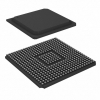
Available in a 144-pin TFBGA (Thin Fine-Pitch Ball Grid Array) or CSPBGA (Chip Scale Package Ball Grid Array) package
Product Advantages
High-density FPGA architecture for complex design implementation
Low-power operation for energy-efficient applications
Flexible I/O configuration for diverse interfacing requirements
Robust thermal and voltage specifications for reliable performance
Key Reasons to Choose This Product
Proven Virtex-II FPGA technology for reliable and high-performance solutions
Scalable design flexibility to accommodate changing application needs
Power-efficient design for extended battery life in portable devices
Comprehensive development tools and ecosystem support from Xilinx
Quality and Safety Features
Industrial-grade component quality and reliability
Compliance with relevant safety and environmental standards
Compatibility
Designed to be compatible with a wide range of embedded systems and application requirements
Application Areas
Suitable for a variety of embedded applications, including industrial automation, medical equipment, telecommunications, and consumer electronics.
Product Lifecycle
The Xilinx XC2V250-4CSG144C is an obsolete product, meaning it is no longer in active production. However, there may be equivalent or alternative models available from Xilinx that can provide similar functionality and performance. Customers are advised to contact our website's sales team for more information on available options and product lifecycle status.
 XC2V250-4FG456IAMDIC FPGA 200 I/O 456FBGA
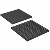 XC2V250-4FGG256IAMDIC FPGA 172 I/O 256FBGA
 XC2V2000-6BGG575CAMDIC FPGA 408 I/O 575BGA
 XC2V2000-6FGG676CAMDIC FPGA 456 I/O 676FBGA
 XC2V2000-6FFG896CAMDIC FPGA 624 I/O 896FCBGA
 XC2V250-4CSG144IAMDIC FPGA 92 I/O 144CSBGA
 XC2V250-4FG456I


