View All

Please refer to the English Version as our Official Version.Return

Europe
France(Français) Germany(Deutsch) Italy(Italia) Russian(русский) Poland(polski) Czech(Čeština) Luxembourg(Lëtzebuergesch) Netherlands(Nederland) Iceland(íslenska) Hungarian(Magyarország) Spain(español) Portugal(Português) Turkey(Türk dili) Bulgaria(Български език) Ukraine(Україна) Greece(Ελλάδα) Israel(עִבְרִית) Sweden(Svenska) Finland(Svenska) Finland(Suomi) Romania(românesc) Moldova(românesc) Slovakia(Slovenská) Denmark(Dansk) Slovenia(Slovenija) Slovenia(Hrvatska) Croatia(Hrvatska) Serbia(Hrvatska) Montenegro(Hrvatska) Bosnia and Herzegovina(Hrvatska) Lithuania(lietuvių) Spain(Português) Switzerland(Deutsch) United Kingdom(English)
Asia/Pacific
Japan(日本語) Korea(한국의) Thailand(ภาษาไทย) Malaysia(Melayu) Singapore(Melayu) Vietnam(Tiếng Việt) Philippines(Pilipino)
Africa, India and Middle East
United Arab Emirates(العربية) Iran(فارسی) Tajikistan(فارسی) India(हिंदी) Madagascar(malaɡasʲ)
South America / Oceania
New Zealand(Maori) Brazil(Português) Angola(Português) Mozambique(Português)
North America
United States(English) Canada(English) Haiti(Ayiti) Mexico(español)
HomeProductsIntegrated Circuits (ICs)PMIC - Voltage Regulators - LinearNCP4623HSN050T1G
NCP4623HSN050T1G Image
Image may be representation.
See specifications for product details.
EXPRESS OPTION
Payment method

NCP4623HSN050T1G - onsemi

Manufacturer Part Number
NCP4623HSN050T1G
Manufacturer
onsemi
Allelco Part Number
32D-NCP4623HSN050T1G
Warranty
1 Year Allelco Warranty - Find out more
Stock Status:
15,500 pcs available, New & Original
Parts Description
IC REG LINEAR 5V 150MA SOT23-5
Package
SOT-23-5
Data sheet
NCP4623HSN050T1.pdf

Datasheets

NCP4623.pdf

PCN Obsolescence/ EOL

Mult Devices EOL 26/Jul/2018.pdf

Environmental Information

onsemi REACH.pdf onsemi RoHS.pdf
RoHs Status
 
Our certification
In stock: 15500

Required fields are indicated by an asterisk (*)
Please send RFQ, we will respond immediately.

Quantity

Specifications

NCP4623HSN050T1G Tech Specifications
onsemi - NCP4623HSN050T1G technical specifications, attributes, parameters and parts with similar specifications to onsemi - NCP4623HSN050T1G

Product Attribute Attribute Value
Manufacturer onsemi
Voltage Dropout (Max) 0.4V @ 20mA
Voltage - Output (Min/Fixed) 5V
Voltage - Output (Max) -
Voltage - Input (Max) 24V
Supplier Device Package SOT-23-5
Series -
Protection Features Over Current, Over Temperature, Short Circuit
Package / Case SC-74A, SOT-753
Package Tape & Reel (TR)
Product Attribute Attribute Value
PSRR 35dB (1kHz)
Output Type Fixed
Output Configuration Positive
Operating Temperature -40°C ~ 85°C
Number of Regulators 1
Mounting Type Surface Mount
Current - Quiescent (Iq) 10 µA
Current - Output 150mA
Control Features Enable
Base Product Number NCP4623

Environmental & Export Classifications

ATTRIBUTE DESCRIPTION
Moisture Sensitivity Level (MSL) 1 (Unlimited)
REACH Status REACH Unaffected
ECCN EAR99
HTSUS 8542.39.0001

Parts Introduction

NCP4623HSN050T1G Image
NCP4623HSN050T1G (1)

Manufacturer Part Number

NCP4623HSN050T1G

Manufacturer

onsemi

Introduction

The NCP4623HSN050T1G is an LDO voltage regulator designed for power management applications.

Product Features and Performance

Low Dropout (LDO) Regulator

Positive Output Configuration

Fixed output voltage of 5V

Supports up to 150mA output current

Very low quiescent current of 10 µA

Excellent Power Supply Rejection Ratio (PSRR) of 35dB at 1kHz

Includes Enable Control Feature

Built-in Protection Features including Over Current, Over Temperature, and Short Circuit

Product Advantages

High efficiency with low voltage dropout of 0.4V at 20mA

Suitable for battery-powered devices due to low Iq

Robust protection features enhance product reliability

NCP4623HSN050T1G Image
NCP4623HSN050T1G (2)

Key Technical Parameters

Maximum Input Voltage: 24V

Minimum/Fixed Output Voltage: 5V

Maximum Voltage Dropout: 0.4V @ 20mA

Output Current Capability: 150mA

Quiescent Current: 10 µA

PSRR: 35dB (1kHz)

Operating Temperature Range: -40°C to 85°C

Quality and Safety Features

Over Current Protection

Over Temperature Protection

Short Circuit Protection

Compatibility

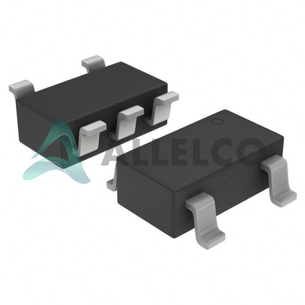
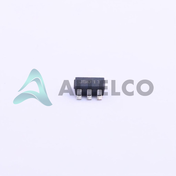
Surface Mount Mounting Type

Compatible with SC-74A, SOT-753 Packages

Application Areas

Consumer Electronics

Mobile Devices

Wireless Communication Systems

Portable Battery-Powered Devices

Product Lifecycle

Obsolete status indicates nearing end of life

Alternatives or upgrades may need to be considered for new designs

Several Key Reasons to Choose This Product

High reliability in various temperature conditions (-40°C to 85°C)

Minimal power loss thanks to the low dropout design

Preserves battery life due to ultra-low quiescent current

Protection features safeguard the device from a range of electrical faults

Ideal for space-constrained applications with its compact SOT-23-5 package

Ease of integration into existing designs with common SC-74A, SOT-753 footprint

Simple enable feature to allow flexible control over power state

Frequently Asked Questions(FAQ)

How does the NCP4623HSN050T1G handle thermal performance under continuous 150mA load conditions, and what are the implications for PCB layout in high-ambient temperature environments?
The NCP4623HSN050T1G features comprehensive over-temperature protection with a typical shutdown threshold around 150°C, ensuring safe operation during thermal stress. Under sustained 150mA output current with a 24V input-to-output differential of 19V, power dissipation reaches approximately 2.85W in the SOT-23-5 package. While internal thermal shutdown prevents catastrophic failure, junction temperatures can exceed 100°C in poorly designed layouts without adequate copper area or airflow. Engineers should allocate at least 10mm² of thermal relief on the PCB’s GND plane beneath the regulator and consider derating output current by 10–15% in ambient temperatures approaching 70°C to maintain margin below thermal limits.
What is the significance of the 0.4V maximum dropout voltage at 20mA, and how does it affect efficiency when powered from a 5.5V source?
The NCP4623HSN050T1G’s 0.4V dropout specification indicates that the minimum required input voltage for stable 5V regulation is 5.4V at light loads. When operating from a 5.5V rail, the dropout margin is only 0.1V, which may push the regulator near its dropout boundary under transient loads or due to tolerance accumulation in both input and reference voltages. This results in reduced headroom for voltage transients, potentially causing output droop. In such configurations, the efficiency drops below 90%, and the device may struggle to maintain regulation if the input dips momentarily below 5.4V—highlighting the need for careful supply stability analysis in battery-powered or low-voltage systems.
Can the NCP4623HSN050T1G be safely used with input voltages exceeding 24V, and what protective mechanisms prevent damage during brief overvoltage events?
No, the absolute maximum input voltage is 24V per datasheet specifications; operation beyond this limit risks permanent device degradation. However, the NCP4623HSN050T1G includes robust internal protection features such as reverse-battery protection and ESD immunity up to ±8kV HBM, which help mitigate damage from occasional voltage spikes. For applications where input transients may briefly exceed 24V (e.g., inductive switching in automotive environments), an external TVS diode rated for 30V clamping should be added in parallel with the input, placed within one inch of the IC, to divert surge energy away from the regulator’s internal circuitry and ensure long-term reliability.
How does the quiescent current of 10 µA influence battery life in portable designs, and what design choices minimize leakage in sleep modes?
With a quiescent current of just 10 µA, the NCP4623HSN050T1G contributes minimally to standby power draw—approximately 0.1 mWh per hour when inactive. This makes it suitable for always-on low-power subsystems like sensor hubs or wake-up circuits. To further reduce leakage, disable the EN pin via a pull-down resistor or microcontroller control rather than leaving it floating. Additionally, placing bypass capacitors close to the VIN and VOUT pins reduces switching noise that could trigger false enable signals. Avoid using ceramic capacitors with high ESR variation across temperature, as they can cause erratic behavior during cold startup—opt instead for X7R dielectrics with stable capacitance over -40°C to 85°C.
In what scenarios would the AP2204K-5.0TRG1 be preferred over the NCP4623HSN050T1G, and how do their protection features compare?
The AP2204K-5.0TRG1 offers similar 5V fixed output but typically includes lower quiescent current (~3 µA) and slightly better dropout performance (~0.35V). It may be favored in ultra-low-power applications where every microamp counts, such as IoT edge nodes with multi-year battery life requirements. Unlike the NCP4623HSN050T1G, which emphasizes over-current, over-temperature, and short-circuit protection, the AP2204K often integrates foldback current limiting and has a more aggressive thermal shutdown response. However, the NCP4623 provides stronger PSRR (35dB vs. ~25dB) and wider input tolerance, making it preferable in noisy industrial environments or where input filtering is minimal.
What impact does the 35dB PSRR at 1kHz have on noise-sensitive analog subcircuits, and how should decoupling be implemented?
A PSRR of 35dB at 1kHz means that power supply ripple at that frequency is attenuated by a factor of about 31.6, reducing it to 1/31.6 of the input noise level. While adequate for most digital logic, this attenuation may be insufficient for precision analog circuits such as ADC references or RF front-end supplies. To improve PSRR, place a 1µF tantalum or film capacitor directly at the VOUT pin and a 0.1µF ceramic capacitor at VIN, both located within 5mm of the regulator. Additionally, use a ferrite bead between the input bulk capacitor and the regulator if higher-frequency noise suppression (>100kHz) is needed, ensuring the bead’s impedance peaks at the dominant noise frequency.
Is the NCP4623HSN050T1G suitable for automotive-grade applications, and what certification or qualification standards apply?
The NCP4623HSN050T1G is not inherently AEC-Q100 qualified, despite its extended commercial temperature range (-40°C to 85°C). It is manufactured using onsemi’s standard semiconductor processes and is intended for industrial or commercial use unless specifically procured through automotive channels with additional screening. For true automotive compliance, components must undergo full qualification including temperature cycling, humidity resistance, and functional validation under ISO/TS 16949 conditions. Therefore, while usable in non-critical automotive peripherals, engineers should verify part number traceability, lot code documentation, and supplier audit reports before deployment in safety-related systems.
How does the SOT-23-5 package footprint affect thermal management in high-density PCBs, and what layout techniques improve heat dissipation?
The SOT-23-5 package measures just 3.0 × 1.6 mm, enabling compact designs but limiting exposed copper for heat spreading. Its thermal resistance from junction to ambient (θJA) is typically 250°C/W in free air, meaning even modest power dissipation causes significant temperature rise. To mitigate this, connect all five pins—especially the GND tab—to a solid ground plane using multiple vias (minimum two 0.3mm vias). Extend thermal pads outward by at least 1mm on all sides and ensure uninterrupted copper pour on adjacent layers. In designs requiring >100mA continuous current, consider adding a small heatsink or relocating the regulator away from other heat sources to maintain junction temperatures well below 125°C.
What role does the Enable pin play in system-level power sequencing, and how can it prevent inrush currents during hot-plug events?
The active-high Enable pin allows external control of the NCP4623HSN050T1G’s output, enabling precise power-up/down sequencing in multi-voltage systems. By asserting EN after the input supply stabilizes and settling transients decay, designers can avoid large inrush currents caused by simultaneous activation of multiple regulators. During hot-plugging, delaying EN assertion by 10–100ms ensures that input capacitors are charged gradually, reducing peak current draw on the source. Conversely, pulling EN low quickly isolates the load from residual charge in output capacitors, preventing backfeeding into the regulator during shutdown—critical in redundant power architectures or battery backup scenarios.
How reliable is the NCP4623HSN050T1G under repetitive thermal cycling, and what failure modes should be anticipated in harsh environments?
The NCP4623HSN050T1G is rated for industrial temperature operation, implying basic robustness against thermal cycling, but it lacks explicit JEDEC JESD22-A104 qualification data. Repeated transitions between -40°C and 85°C accelerate solder joint fatigue at the SOT-23-5 bond wires and leadframe interface. Primary failure modes include open connections due to coefficient of thermal expansion mismatch and parametric drift in reference voltage over time. To enhance longevity, avoid rapid thermal swings during assembly (e.g., reflow soldering) by confirming MSL compatibility (this part is MSL 1) and storing unused devices in dry ambient conditions. Also, minimize mechanical stress during board handling by securing the package near the center of the pad field.
What are the key differences between the NCP4623HSN050T1G and the base product NCP4623 family variants in terms of output voltage options and packaging availability?
The base NCP4623 series supports adjustable output versions (via external resistors) in addition to fixed outputs like the NCP4623HSN050T1G’s 5V variant. Other fixed-voltage models include 3.3V, 1.8V, and 1.5V options, each optimized for specific rail requirements. All share the same SOT-23-5 package and core protection features, but dropout voltage and Iq vary slightly across variants. For example, the 1.5V version may exhibit lower dropout due to reduced internal bias current, improving efficiency in low-voltage applications. Engineers selecting between variants should prioritize matching the output voltage to system rails while considering trade-offs in noise performance and quiescent consumption based on application duty cycle.
How does the short-circuit protection mechanism operate, and what recovery behavior follows a fault condition?
Upon detecting an output short, the NCP4623HSN050T1G activates internal current limiting that typically clamps output current to around 150mA to 200mA, depending on layout and temperature. After approximately 100ms of continuous overcurrent, the device enters hiccup mode—cycling on and off repeatedly until the fault is removed. This prevents thermal runaway while allowing automatic recovery once the short is cleared. However, repeated shorting under poor ventilation may still accumulate enough energy to trigger overtemperature shutdown before hiccup initiates. Designers should ensure adequate airflow or add a current-sense resistor upstream for faster fault detection if instantaneous disconnection is required.
Can the NCP4623HSN050T1G regulate efficiently when used with switching pre-regulators in distributed power architectures?
Yes, when paired with a buck converter upstream, the NCP4623HSN050T1G can provide clean, low-noise 5V rails for sensitive loads. The buck output acts as the regulated input, reducing the linear regulator’s dropout burden and improving overall efficiency—especially beneficial when the input voltage varies widely (e.g., 12V to 18V). In such configurations, the linear stage primarily filters high-frequency switching ripple, leveraging the regulator’s decent PSRR above 100kHz. However, ensure the buck output is sufficiently filtered with LC networks to meet the NCP4623’s input ripple specifications (<50mVpp), otherwise PSRR degradation will compromise output quality.
What considerations apply when replacing the NCP4623HSN050T1G with the AP2204K-5.0TRG1 in existing designs, particularly regarding pin compatibility and thermal characteristics?
Both the NCP4623HSN050T1G and AP2204K-5.0TRG1 use the SOT-23-5 package and identical pinout (VIN, EN, GND, NC, VOUT), enabling direct substitution in footprint-constrained layouts. However, the AP2204K operates at lower quiescent current (3 µA vs. 10 µA) and has slightly tighter output voltage tolerance (±2% vs. ±3%), improving accuracy in precision analog paths. Thermally, both packages exhibit similar θJA, so no significant layout changes are needed unless ambient conditions approach 80°C. Still, verify that the AP2204K’s shorter response time to load transients meets timing requirements, as some versions lack built-in soft-start and may overshoot during step-load events compared to the NCP4623’s more controlled turn-on profile.
How does moisture sensitivity level (MSL) classification impact storage and handling of the NCP4623HSN050T1G, and what precautions apply during reflow soldering?
Classified as MSL 1 (Unlimited), the NCP4623HSN050T1G requires no special drying prior to use and can remain indefinitely in standard storage conditions (≤30°C, <80% RH) without baking. During PCB assembly, adhere to standard JEDEC J-STD-020C reflow profiles: peak temperature ≤260°C for ≤10 seconds. Exceeding these limits risks delamination at the mold compound-semiconductor interface, especially given the thin die attach layer in SOT-23 packages. Always store unpackaged units in sealed bags with desiccant until immediate use. Label trays and reels with humidity indicators to monitor exposure, particularly in humid climates where condensation during dewarping could compromise reliability.
What are the implications of the EAR99 classification for international sourcing and export control compliance?
As an EAR99 component, the NCP4623HSN050T1G is generally exempt from strict U.S. export controls unless integrated into defense or space systems. However, end-use restrictions may apply if the final product is destined for embargoed regions or military applications. Importers must still comply with local regulations, such as China’s ML category rules or EU dual-use controls. While procurement complexity is minimal for commercial electronics, engineers should document intended use clearly in purchase orders and avoid mislabeling shipments as “civilian” when the product contains any controlled technology, however minor.
How does the enable feature interact with brown-out conditions, and what logic levels guarantee reliable activation?
The NCP4623HSN050T1G accepts enable logic levels down to 1.0V, ensuring compatibility with low-voltage microcontrollers even when the input rail is near dropout. During brown-out events (input voltage falling below 5.4V), the regulator may enter dropout, but the enable signal remains unaffected—allowing the MCU to assert EN independently. To prevent false triggering from slow-rising inputs, add hysteresis via a simple RC network on the EN pin or use a dedicated supervisor IC. Ensure EN assertion occurs only after VIN exceeds 3.0V to avoid undefined states, and confirm that the controlling GPIO can sink/source at least 1µA to override internal leakage reliably.
What testing methodology best validates the NCP4623HSN050T1G’s performance under real-world transient loads, and what instrumentation is recommended?
Use a programmable electronic load capable of simulating 0–150mA steps (e.g., 10µs rise/fall times) combined with a mixed-signal oscilloscope to capture output voltage deviations. Inject transients mimicking motor starts, USB enumeration, or RF transmit bursts, and measure recovery time (<50µs for <100mV droop). Simultaneously log junction temperature via thermocouple attached to the package backside using conductive epoxy. Include input ripple measurement with a high-bandwidth differential probe to assess PSRR effectiveness. Automate sequences using LabVIEW or Python scripts to repeat tests across temperature extremes, capturing statistical distributions of dropout voltage and Iq variations for robust qualification reporting.

Parts with Similar Specifications

The three parts on the right have similar specifications to onsemi NCP4623HSN050T1G

Product Attribute NCP4623HSN100T1G NCP4623HSN120T1G NCP4623HSNADJT1G NCP4623HMX050TCG
Part Number NCP4623HSN100T1G NCP4623HSN120T1G NCP4623HSNADJT1G NCP4623HMX050TCG
Manufacturer onsemi onsemi onsemi onsemi
Voltage - Input (Max) - - - -
Voltage - Output (Min/Fixed) - - - -
Voltage - Output (Max) - - - -
Number of Regulators - - - -
Base Product Number - DAC34H84 MAX500 ADS62P42
Output Type - Current - Unbuffered Voltage - Buffered -
Package - Tape & Reel (TR) Tube Tape & Reel (TR)
Mounting Type - Surface Mount Through Hole Surface Mount
Voltage Dropout (Max) - - - -
Package / Case - 196-LFBGA 16-DIP (0.300', 7.62mm) 64-VFQFN Exposed Pad
Output Configuration - - - -
Current - Quiescent (Iq) - - - -
Protection Features - - - -
Series - - - -
PSRR - - - -
Current - Output - - - -
Control Features - - - -
Operating Temperature - -40°C ~ 85°C 0°C ~ 70°C -40°C ~ 85°C
Supplier Device Package - 196-NFBGA (12x12) 16-PDIP 64-VQFN (9x9)

NCP4623HSN050T1G Datasheet PDF

Download NCP4623HSN050T1G pdf datasheets and onsemi documentation for NCP4623HSN050T1G - onsemi.

Datasheets
NCP4623.pdf
PCN Obsolescence/ EOL
Mult Devices EOL 26/Jul/2018.pdf
Environmental Information
onsemi REACH.pdf onsemi RoHS.pdf

Customer Reviews

Evaluation: 10 Articles

  • Dani***alkerTech
    Jun 1, 2026

    Product works, but setup took more effort than expected. Once configured the MCU ran reliably, although documentation support felt older compared with newer platforms. Fine for maintenance projects.

  • Yuki***aka88
    May 26, 2026

    信号通信プロジェクトでこのRS-485トランシーバーを使用しました。設置は簡単で、長距離ケーブルでも通信は安定していました。消費電力も、以前使用していたものより低くなっています。

  • Stev***aker
    May 20, 2026

    Solid diode for power rectification. Works well in switching circuits.

  • Bran***Lewis
    May 11, 2026

    Compact FPGA with good performance. Suitable for basic signal processing tasks.

  • Oliv***arris
    May 7, 2026

    Reliable I/O expander. Works well in embedded control applications.

  • Jess***Jones
    Apr 17, 2026

    It offers good value for the price, and the specifications match the description. I’ve been using it for two days with no issues, and I’ll definitely buy it again if I need it in the future.

  • Mich***Smith
    Apr 17, 2026

    Shipping was on time, the component pins are neatly aligned, and I tested 10 of them with a multimeter—all readings were within the specified range. Highly recommended.

  • Aman***arris
    Apr 3, 2026

    It was great—the entire process, from placing the order to receiving the package, went very smoothly. The components were consistent, the price was fair, and I had a very pleasant shopping experience.

  • Mike***nch
    Apr 3, 2026

    Better than expected! The resistance and capacitance readings were spot-on, and it passed the test on the first try. The service was reliable, and the packaging was thoughtful—I highly recommend it.

  • Daic***K.
    Mar 23, 2026

    Very good. No issue after long time testing.

Write a Review

Your Email address will not be published.

Shipment

Delivery Time

In-stock items can be shipped within 24 hours. Some parts will be arranged for delivery within 1-2 days from the date all items arrive at our warehouse. And Allelco ships order once a day at about 17:00, except Sunday. Once the goods are shipped, the estimated delivery time depends on the shipping methods and Delivery destination. The table below shows are the logistic time for some common countries.

Delivery Cost

  1. Use your express account for shipment if you have one.
  2. Use our account for the shipment. Refer to the table below for the approximate charges.
(Different time frame / countries / package size has different price.)

Delivery Method

  1. Global Common Shipment by DHL / UPS / FedEx / TNT / EMS / SF we support.
  2. Others more shipping ways, please get in touch with your customer manager.

Common Countries Logistic Time Reference
Region Country Logistic Time(Day)
America United States 5
Brazil 7
Europe Germany 5
United Kingdom 4
Italy 5
Oceania Australia 6
New Zealand 5
Asia India 4
Japan 4
Middle East Israel 6
DHL & FedEx Shipment Charges Reference
Shipment charges(KG) Reference DHL(USD$)
0.00kg-1.00kg USD$30.00 - USD$60.00
1.00kg-2.00kg USD$40.00 - USD$80.00
2.00kg-3.00kg USD$50.00 - USD$100.00
Note:
The above table is for reference only. There may have some data bias for the uncontrollable factors.
Contact us if you have any questions.
  • QC (Quality Warranty)
  • Payment Support
  • Packaging
  • Certifications & Memberships

QC (Quality Warranty)

Allelco is committed to exceeding customer expectations through customer service excellence, order accuracy, and on-time delivery.
This is achieved through our commitment to the continual improvement of our processes, services, and products.


Strict quality inspection builds a solid foundation for electronic component quality.
  1. Visual inspection
  2. Performance testing and reliability verification
  3. Standardized full-process testing
  4. Precise control of every parameter
We eliminate defective components and ensure the stable operation of electronic devices through professional quality standards.

Payment Support

The payment method can be chosen from the methods shown below: Wire Transfer (T/T, Bank Transfer), Western Union, Credit card, PayPal.
  • HKBea
  • Paypal
  • MasterCard
  • Western-Union
  • VISA
Stable Delivery, Sincere Partnership — Your Faithful Supply Chain Partner
  • Efficient Supply Management
  • Cost-Saving Procurement
  • Fast Sourcing & Delivery
Contact us if you have any questions.

Packaging

Electrostatic Discharge Protection and Handling

All electrostatic-sensitive components are handled in accordance with electrostatic discharge control procedures. The products are hermetically sealed in anti-static safe packaging to prevent electrostatic damage. Appropriate labeling is also applied for identification and traceability. This ensures product integrity during storage, handling and transportation.


ESD

Certifications & Memberships

Third-party certified, strict quality control. Our certification
  • ISO 9001: 2015
  • ISO 13485: 2016
  • ISO 14001: 2015
  • ISO 28000: 2007
  • ISO 45001: 2018
  • GB/T 27922-2011
  • SMTA
  • IPC
  • ESD
  • PSMA
NCP4623HSN050T1G Image

NCP4623HSN050T1G

onsemi
32D-NCP4623HSN050T1G

Want a better price? Add to Cart and Submit RFQ now, we'll contact you immediately.

0 RFQ
Shopping cart (0 Items)
It is empty.
Compare List (0 Items)
It is empty.
Feedback

Your feedback matters! At Allelco, we value the user experience and strive to improve it constantly.
Please share your comments with us via our feedback form, and we'll respond promptly.
Thank you for choosing Allelco.

Subject
E-mail
Comments
Captcha
Drag or click to upload file
Upload File
types: .xls, .xlsx, .doc, .docx, .jpg, .png and .pdf.
Max file size: 10MB