


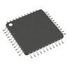
 ATMEGA8515L-8AIMicrochip TechnologyIC MCU 8BIT 8KB FLASH 44TQFP
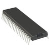 ATMEGA8515L-8PCMicrochip TechnologyIC MCU 8BIT 8KB FLASH 40DIP
 ATMEGA8515L-8MUAtmelIC MCU 8BIT 8KB FLASH 44VQFN
- Dani***alkerTech
- Jun 1, 2026
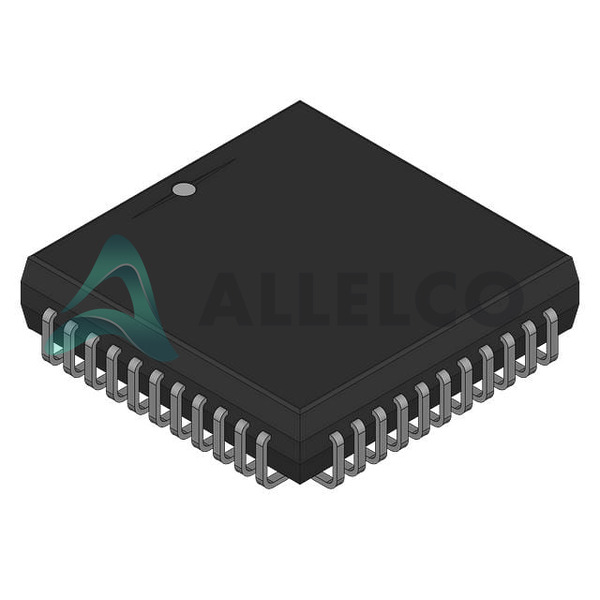

Image may be representation.
See specifications for product details.
See specifications for product details.
- EXPRESS OPTION
- Payment method
ATMEGA8515L-8JU - Atmel
- Manufacturer Part Number
- ATMEGA8515L-8JU
- Manufacturer
- Atmel
- Allelco Part Number
- 32D-ATMEGA8515L-8JU
- Warranty
- 1 Year Allelco Warranty - Find out more
- Stock Status:
- 13,530 pcs available, New & Original
- Parts Description
- IC MCU 8BIT 8KB FLASH 44PLCC
- Package
- 44-PLCC (16.6x16.6)
- Data sheet
- -
- RoHs Status
- Our certification
- In stock: 13530
- Unit Price: $5.141
- Subtotal: $0.00
Want a better price?
Add to Cart and Submit RFQ now, we'll contact you immediately.
| Quantity | Unit Price | Ext. Price |
|---|---|---|
| 1+ | $5.141 | $5.14 |
| 10+ | $4.909 | $49.09 |
| 30+ | $4.769 | $143.07 |
| 100+ | $4.651 | $465.10 |
The above prices does not include taxes and freight rates, which will be calculated on the order pages.


