View All

Please refer to the English Version as our Official Version.Return

Europe
France(Français) Germany(Deutsch) Italy(Italia) Russian(русский) Poland(polski) Czech(Čeština) Luxembourg(Lëtzebuergesch) Netherlands(Nederland) Iceland(íslenska) Hungarian(Magyarország) Spain(español) Portugal(Português) Turkey(Türk dili) Bulgaria(Български език) Ukraine(Україна) Greece(Ελλάδα) Israel(עִבְרִית) Sweden(Svenska) Finland(Svenska) Finland(Suomi) Romania(românesc) Moldova(românesc) Slovakia(Slovenská) Denmark(Dansk) Slovenia(Slovenija) Slovenia(Hrvatska) Croatia(Hrvatska) Serbia(Hrvatska) Montenegro(Hrvatska) Bosnia and Herzegovina(Hrvatska) Lithuania(lietuvių) Spain(Português) Switzerland(Deutsch) United Kingdom(English)
Asia/Pacific
Japan(日本語) Korea(한국의) Thailand(ภาษาไทย) Malaysia(Melayu) Singapore(Melayu) Vietnam(Tiếng Việt) Philippines(Pilipino)
Africa, India and Middle East
United Arab Emirates(العربية) Iran(فارسی) Tajikistan(فارسی) India(हिंदी) Madagascar(malaɡasʲ)
South America / Oceania
New Zealand(Maori) Brazil(Português) Angola(Português) Mozambique(Português)
North America
United States(English) Canada(English) Haiti(Ayiti) Mexico(español)
HomeProductsDiscrete Semiconductor ProductsDiodes - RFHSMP-3812-TR1G
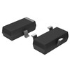
HSMP-3812-TR1G Image
Image may be representation.
See specifications for product details.
EXPRESS OPTION
Payment method

HSMP-3812-TR1G - Broadcom Limited

Manufacturer Part Number
HSMP-3812-TR1G
Manufacturer
Avago Technologies (Broadcom)
Allelco Part Number
32D-HSMP-3812-TR1G
Warranty
1 Year Allelco Warranty - Find out more
Stock Status:
4,170 pcs available, New & Original
Parts Description
RF DIODE PIN 100V SOT23-3
Package
SOT-23-3
Data sheet
HSMP-3812-TR1G.pdf

Datasheets

HSMP-381x, 481x.pdf
RoHs Status
 
Our certification
In stock: 4170

Required fields are indicated by an asterisk (*)
Please send RFQ, we will respond immediately.

Quantity

Specifications

HSMP-3812-TR1G Tech Specifications
Broadcom Limited - HSMP-3812-TR1G technical specifications, attributes, parameters and parts with similar specifications to Broadcom Limited - HSMP-3812-TR1G

Product Attribute Attribute Value
Manufacturer Avago Technologies (Broadcom)
Voltage - Peak Reverse (Max) 100V
Supplier Device Package SOT-23-3
Series -
Resistance @ If, F 3Ohm @ 100mA, 100MHz
Package / Case TO-236-3, SC-59, SOT-23-3
Product Attribute Attribute Value
Package Tape & Reel (TR)
Operating Temperature 150°C (TJ)
Diode Type PIN - 1 Pair Series Connection
Current - Max 1 A
Capacitance @ Vr, F 0.35pF @ 50V, 1MHz
Base Product Number HSMP-3812

Environmental & Export Classifications

ATTRIBUTE DESCRIPTION
Moisture Sensitivity Level (MSL) 1 (Unlimited)
REACH Status REACH Unaffected
ECCN EAR99
HTSUS 8541.10.0080

Parts Introduction

HSMP-3812-TR1G Image
HSMP-3812-TR1G (1)

Manufacturer Part Number

HSMP-3812-TR1G

Manufacturer

Broadcom

Introduction

The HSMP-3812-TR1G is a RF diode from Broadcom, a leading manufacturer of semiconductor components. This diode features a PIN (Positive-Intrinsic-Negative) configuration with a series connection, making it suitable for a variety of RF and microwave applications.

Product Features and Performance

Peak Reverse Voltage (Max): 100V

Maximum Current: 1A

Capacitance @ Vr, F: 0.35pF @ 50V, 1MHz

Resistance @ If, F: 3Ohm @ 100mA, 100MHz

Operating Temperature: 150°C (TJ)

Package: TO-236-3, SC-59, SOT-23-3

Product Advantages

Compact and space-saving package options

High-performance characteristics suitable for RF and microwave applications

Reliable and durable construction for demanding operating conditions

Key Reasons to Choose This Product

Proven reliability and performance from a trusted manufacturer

Versatile design suitable for a wide range of RF and microwave applications

Cost-effective solution for projects with tight budgets or space constraints

Quality and Safety Features

Rigorous quality control and testing procedures

Compliance with industry safety and environmental standards

Compatibility

The HSMP-3812-TR1G is a direct replacement for the HSMP-3812 base product number.

Application Areas

RF and microwave circuits

Wireless communication systems

Test and measurement equipment

Industrial and military applications

Product Lifecycle

The HSMP-3812-TR1G is an obsolete product, meaning it is no longer in active production. However, there may be equivalent or alternative models available from Broadcom or other manufacturers. Customers are advised to contact our website's sales team for more information on suitable replacement options.

Frequently Asked Questions(FAQ)

What is the typical application circuit for the HSMP-3812-TR1G PIN diode in high-frequency switching scenarios, and how does its capacitance profile support such use?
The HSMP-3812-TR1G is optimized for RF switch and attenuator circuits operating above 1 GHz due to its ultra-low junction capacitance of 0.35 pF at 50 V bias and 1 MHz. This low capacitance minimizes insertion loss and preserves signal integrity in transmit/receive (T/R) modules. In a typical SPDT configuration, the pair-connected diodes enable fast switching between paths with minimal charge storage effects. The 3 Ω dynamic resistance under 100 mA forward current further supports efficient turn-on characteristics during switching transitions, making it suitable for radar and communication systems where isolation and linearity are critical.
How does the HSMP-3812-TR1G compare to the SMP1307-005LF in terms of reverse recovery time and suitability for high-speed RF switching applications?
While both the HSMP-3812-TR1G and SMP1307-005LF serve similar PIN diode roles, the HSMP-3812 offers superior performance in high-power RF environments due to its 1 A forward current rating and 100 V peak reverse voltage. Although neither device has a formal reverse recovery time specified—being majority-carrier devices—the HSMP-3812’s lower series resistance and optimized epitaxial layer design yield faster switching transients compared to the SMP1307. This makes the HSMP-3812-TR1G more appropriate for pulsed radar and wideband amplifier protection circuits requiring minimal latency during switching.
What design considerations are necessary when integrating the HSMP-3812-TR1G into a microstrip-based RF switch to prevent thermal derating issues?
Thermal management is essential when using the HSMP-3812-TR1G in microstrip switches due to its maximum junction temperature of 150°C. In compact SOT-23-3 packages, localized heating can reduce effective power handling. Designers should ensure adequate copper area on the PCB for heat dissipation, especially during continuous-wave (CW) operation. A typical rule of thumb is to limit average forward current to less than 500 mA in ambient temperatures above 60°C unless thermal vias connect the pad to an internal ground plane. Without such measures, elevated package temperature may increase series resistance and degrade switching performance over time.
Can the HSMP-3812-TR1G be used in DC blocking or biasing applications, and what limitations apply regarding DC current handling?
Yes, the HSMP-3812-TR1G can function as a DC block in RF links due to its inherent reverse-biased junction capacitance, which presents high impedance at low frequencies. However, it cannot conduct significant DC current in the forward direction beyond its 1 A rating. When used in bias-T applications, the device must be reverse-biased to avoid loading the DC supply. Careful attention to lead inductance and parasitic capacitance in layout is required to prevent unintended RF coupling or resonance near the cutoff frequency determined by C₀ = 0.35 pF.
What is the impact of bias voltage on the HSMP-3812-TR1G’s capacitance, and how does this influence insertion loss in variable attenuators?
The HSMP-3812-TR1G exhibits a nonlinear capacitance-voltage relationship typical of PIN diodes, where increasing reverse bias reduces junction capacitance. At zero bias, capacitance rises slightly due to diffusion effects, but remains below 0.4 pF up to 50 V reverse voltage. In a reflective-type attenuator, this variation enables precise control of attenuation depth through bias applied to the HSMP-3812. For example, toggling between -5 V and +10 mA bias changes the impedance seen by the RF signal, modulating path loss from approximately 0.5 dB to 20 dB depending on matching network design. This makes the component effective for digitally controlled level adjustment in test equipment.
How does the HSMP-3812-TR1G perform in terms of isolation when configured in a shunt mode within a T/R switch, and what factors limit its effectiveness?
In shunt-mode operation, the HSMP-3812-TR1G provides moderate isolation, typically exceeding 25 dB at 2 GHz, limited primarily by its finite series resistance and residual capacitance. Isolation degrades with increasing frequency due to capacitive coupling through C₀ = 0.35 pF, especially when biased lightly or at DC. Additionally, package parasitics and trace inductance in the RF path can resonate with the diode’s input impedance, reducing off-state rejection. Proper grounding, short lead lengths, and careful PCB layout are therefore critical to maintaining isolation above 30 dB in practical implementations.
What are the key differences between the HSMP-3812-TR1G and BAR66E6327HTSA1 in terms of package type, power handling, and high-frequency behavior?
The HSMP-3812-TR1G uses a compact SOT-23-3 package and supports up to 1 A forward current with 100 V reverse rating, whereas the BAR66E6327HTSA1 is housed in a larger SOD-323 package and typically rated for lower current (~150 mA). Despite similar voltage ratings, the HSMP-3812’s lower series resistance (3 Ω @ 100 MHz) gives it better conduction efficiency at higher currents, making it preferable for high-power switching. However, the BAR66 variant may offer slightly lower capacitance due to different epitaxial structures, potentially benefiting ultra-wideband applications below 500 MHz.
How should the HSMP-3812-TR1G be mounted and routed on a PCB to minimize RF losses and ensure reliable performance in 5G front-end modules?
To optimize performance in 5G front-end modules, the HSMP-3812-TR1G should be surface-mounted directly onto the RF ground plane using a solid solder pad aligned with the SOT-23-3 footprint. Lead lengths must be minimized—ideally less than 1 mm—to reduce parasitic inductance that could resonate with C₀ around 1.5 GHz. The cathode and anode traces should follow a straight-line path without sharp bends, and the bias line should be isolated from RF signals to prevent feedthrough. Thermal relief is unnecessary unless cooling is actively managed, as MSL Level 1 ensures robustness against moisture during assembly.
What testing methodology is recommended to validate the HSMP-3812-TR1G’s performance in a real-world RF switch before full production release?
A recommended validation approach involves building a prototype SPDT switch using the HSMP-3812-TR1G with microstrip transmission lines matched to 50 Ω. Key metrics include measuring insertion loss (< 0.8 dB at 2–6 GHz), isolation (> 25 dB), return loss (> 15 dB), and VSWR across the band using a vector network analyzer (VNA). Bias sweep tests from -10 V to +100 mA should confirm monotonic control of attenuation. Thermal cycling between -40°C and +125°C followed by RF performance checks ensures reliability under environmental stress, particularly important given the TJmax of 150°C.
Does the HSMP-3812-TR1G require external protection circuitry when used in unidirectional RF power detection applications?
While not strictly mandatory, adding clamping diodes or TVS devices near the HSMP-3812-TR1G improves robustness against ESD events, especially in field-deployed systems. As a PIN diode sensitive to electrostatic discharge, the HSMP-3812 can tolerate standard human-body model (HBM) levels per JEDEC, but cumulative exposure over time may degrade performance. In high-power detection scenarios where reflected energy exceeds 30 dBm, a series resistor or limiting circuit upstream of the HSMP-3812 helps prevent overdrive conditions that could alter its I/V curve permanently.
How does the HSMP-3812-TR1G’s forward voltage drop behave under pulsed versus continuous operation, and what implications exist for power dissipation calculations?
Under continuous DC conditions, the HSMP-3812 exhibits a typical forward voltage drop of 1.2 V at 100 mA. However, during short-duration RF pulses (e.g., 10 µs pulses at 1 kHz duty cycle), the forward voltage decreases slightly due to reduced carrier lifetime effects, lowering instantaneous power dissipation. Designers must account for this difference when calculating average power loss: P_avg = I_f × V_f × D, where D is duty cycle. For pulsed loads common in radar, conservatively assuming V_f ≈ 1.1 V at 1 A still ensures margin against thermal runaway.
Are there any known interoperability issues between the HSMP-3812-TR1G and common RF ICs like GaAs PAs when used in switch control interfaces?
Compatibility generally exists, but level-shifting may be needed if the HSMP-3812’s bias requirements conflict with the output swing of control logic (e.g., 3.3 V CMOS driving a -5 V bias pin). Since the HSMP-3812 operates with both positive and negative bias in active regions, interfacing directly with digital signals risks incorrect state operation. A pull-down resistor and Zener clamp on the bias line are often added to protect against overvoltage. Additionally, ensure that control timing aligns with the HSMP-3812’s soft-switching nature to avoid shoot-through in complementary configurations.
What environmental certifications or compliance marks apply to the HSMP-3812-TR1G, and how do they affect global deployment?
The HSMP-3812-TR1G complies with REACH regulations (Unaffected status), RoHS directives, and is classified under ECCN EAR99 for export control ease. Its HTSUS code (8541.10.0080) facilitates customs clearance in the U.S., while MSL Level 1 indicates no special storage requirements beyond standard dry packaging. These attributes simplify sourcing and distribution across North America, Europe, and Asia without additional screening or documentation, supporting rapid prototyping and mass production timelines.
How does the HSMP-3812-TR1G’s resistance vary with frequency, and why is this relevant for impedance matching networks?
The HSMP-3812-TR1G displays a frequency-dependent resistance characteristic: 3 Ω at 100 MHz under 100 mA bias, increasing slightly at higher frequencies due to skin effect and parasitic inductance. In impedance matching circuits—such as L-networks used in attenuators—this resistive component shifts the load impedance seen by the source, affecting bandwidth and return loss. Accurate modeling requires including R_dyn in simulations; neglecting it can lead to mismatched designs where measured return loss deviates by more than 2 dB from predictions, particularly above 5 GHz.
What precautions should be taken when substituting the HSMP-3812-TR1G with alternative models like MADP-007167-0287DT in existing RF designs?
Substitution demands careful evaluation of electrical parameters beyond basic voltage and current ratings. For instance, MADP-007167-0287DT may have higher capacitance or different epitaxial thickness, altering insertion loss and isolation in the HSMP-3812’s target frequency range. Always re-measure key metrics post-substitution using calibrated test fixtures. Layout compatibility is also critical—different package outlines may necessitate redesign of RF traces or bias routing. Documentation updates and change-control records should accompany any substitution to maintain traceability in safety-critical systems.
Why might the HSMP-3812-TR1G exhibit non-ideal behavior in very low-power receive chains despite its favorable specifications?
At extremely low signal levels (below -60 dBm), the HSMP-3812’s series resistance (3 Ω) and residual capacitance (0.35 pF) create a small but non-negligible insertion loss floor, limiting sensitivity. Moreover, leakage currents and bias-induced standing waves can dominate noise performance in high-impedance front ends. In such cases, even minor mismatches cause disproportionate degradation in SNR. Adding pre-matching stages or selecting diodes with lower Q-factor alternatives may improve performance, though trade-offs in size, cost, and linearity must be evaluated against system requirements.

Parts with Similar Specifications

The three parts on the right have similar specifications to Broadcom Limited HSMP-3812-TR1G

Product Attribute HSMP-3812-TR2G HSMP-3810-TR1G HSMP-3812-TR1 HSMP-3813-TR1G
Part Number HSMP-3812-TR2G HSMP-3810-TR1G HSMP-3812-TR1 HSMP-3813-TR1G
Manufacturer Broadcom Limited Broadcom Limited Broadcom Limited Broadcom Limited
Diode Type - - - -
Current - Max - - - -
Voltage - Peak Reverse (Max) - - - -
Resistance @ If, F - - - -
Supplier Device Package - 196-NFBGA (12x12) 16-PDIP 64-VQFN (9x9)
Package / Case - 196-LFBGA 16-DIP (0.300', 7.62mm) 64-VFQFN Exposed Pad
Base Product Number - DAC34H84 MAX500 ADS62P42
Series - - - -
Operating Temperature - -40°C ~ 85°C 0°C ~ 70°C -40°C ~ 85°C
Package - Tape & Reel (TR) Tube Tape & Reel (TR)
Capacitance @ Vr, F - - - -

HSMP-3812-TR1G Datasheet PDF

Download HSMP-3812-TR1G pdf datasheets and Broadcom Limited documentation for HSMP-3812-TR1G - Broadcom Limited.

Datasheets
HSMP-381x, 481x.pdf

Customer Reviews

Evaluation: 10 Articles

  • Nord***mbedded
    Jul 20, 2026

    Reliable FPGA with predictable behavior. Configuration and testing went smoothly, making development faster than expected.

  • Arch***ct
    Jul 15, 2026

    Used this device in a communication signal processing board. Stable timing and no unexpected issues during implementation.

  • FPGA***lorer88
    Jul 7, 2026

    The FPGA works properly and all functions operate as expected. Documentation required some additional research, but overall it is a usable device for smaller signal processing projects.

  • Nath***oleman
    Jun 29, 2026

    Used this sensor component in an industrial automation setup. Detection accuracy was consistent and installation was straightforward.

  • Emil***rperTech
    Jun 23, 2026

    Works exactly as described. I used it as a USB-to-SPI bridge in a small MCU development project and communication was stable from the first setup.

  • Liam***terTech
    Jun 15, 2026

    Used this CPLD in a logic control project. Programming was straightforward and signal timing matched the design requirements.

  • Nath***rooks
    Jun 11, 2026

    Installed this power component in a converter board. Output remained stable under different load conditions and thermal performance was better than expected.

  • Dani***alkerTech
    Jun 1, 2026

    Product works, but setup took more effort than expected. Once configured the MCU ran reliably, although documentation support felt older compared with newer platforms. Fine for maintenance projects.

  • Yuki***aka88
    May 26, 2026

    信号通信プロジェクトでこのRS-485トランシーバーを使用しました。設置は簡単で、長距離ケーブルでも通信は安定していました。消費電力も、以前使用していたものより低くなっています。

  • Stev***aker
    May 20, 2026

    Solid diode for power rectification. Works well in switching circuits.

Write a Review

Your Email address will not be published.

Shipment

Delivery Time

In-stock items can be shipped within 24 hours. Some parts will be arranged for delivery within 1-2 days from the date all items arrive at our warehouse. And Allelco ships order once a day at about 17:00, except Sunday. Once the goods are shipped, the estimated delivery time depends on the shipping methods and Delivery destination. The table below shows are the logistic time for some common countries.

Delivery Cost

  1. Use your express account for shipment if you have one.
  2. Use our account for the shipment. Refer to the table below for the approximate charges.
(Different time frame / countries / package size has different price.)

Delivery Method

  1. Global Common Shipment by DHL / UPS / FedEx / TNT / EMS / SF we support.
  2. Others more shipping ways, please get in touch with your customer manager.

Common Countries Logistic Time Reference
Region Country Logistic Time(Day)
America United States 5
Brazil 7
Europe Germany 5
United Kingdom 4
Italy 5
Oceania Australia 6
New Zealand 5
Asia India 4
Japan 4
Middle East Israel 6
DHL & FedEx Shipment Charges Reference
Shipment charges(KG) Reference DHL(USD$)
0.00kg-1.00kg USD$30.00 - USD$60.00
1.00kg-2.00kg USD$40.00 - USD$80.00
2.00kg-3.00kg USD$50.00 - USD$100.00
Note:
The above table is for reference only. There may have some data bias for the uncontrollable factors.
Contact us if you have any questions.
  • QC (Quality Warranty)
  • Payment Support
  • Packaging
  • Certifications & Memberships

QC (Quality Warranty)

Allelco is committed to exceeding customer expectations through customer service excellence, order accuracy, and on-time delivery.
This is achieved through our commitment to the continual improvement of our processes, services, and products.


Strict quality inspection builds a solid foundation for electronic component quality.
  1. Visual inspection
  2. Performance testing and reliability verification
  3. Standardized full-process testing
  4. Precise control of every parameter
We eliminate defective components and ensure the stable operation of electronic devices through professional quality standards.

Payment Support

The payment method can be chosen from the methods shown below: Wire Transfer (T/T, Bank Transfer), Western Union, Credit card, PayPal.
  • HKBea
  • Paypal
  • MasterCard
  • Western-Union
  • VISA
Stable Delivery, Sincere Partnership — Your Faithful Supply Chain Partner
  • Efficient Supply Management
  • Cost-Saving Procurement
  • Fast Sourcing & Delivery
Contact us if you have any questions.

Packaging

Electrostatic Discharge Protection and Handling

All electrostatic-sensitive components are handled in accordance with electrostatic discharge control procedures. The products are hermetically sealed in anti-static safe packaging to prevent electrostatic damage. Appropriate labeling is also applied for identification and traceability. This ensures product integrity during storage, handling and transportation.


ESD

Certifications & Memberships

Third-party certified, strict quality control. Our certification
  • ISO 9001: 2015
  • ISO 13485: 2016
  • ISO 14001: 2015
  • ISO 28000: 2007
  • ISO 45001: 2018
  • GB/T 27922-2011
  • SMTA
  • IPC
  • ESD
  • PSMA
HSMP-3812-TR1G Image

HSMP-3812-TR1G

Broadcom Limited
32D-HSMP-3812-TR1G

Want a better price? Add to Cart and Submit RFQ now, we'll contact you immediately.

0 RFQ
Shopping cart (0 Items)
It is empty.
Compare List (0 Items)
It is empty.
Feedback

Your feedback matters! At Allelco, we value the user experience and strive to improve it constantly.
Please share your comments with us via our feedback form, and we'll respond promptly.
Thank you for choosing Allelco.

Subject
E-mail
Comments
Captcha
Drag or click to upload file
Upload File
types: .xls, .xlsx, .doc, .docx, .jpg, .png and .pdf.
Max file size: 10MB