
CY62137CVSL-70BAI (1)
Manufacturer Part Number
CY62137CVSL-70BAI
Manufacturer
Infineon Technologies
Introduction
High-speed 2Mbit Static RAM with parallel interface
Product Features and Performance
Volatile memory technology
Asynchronous SRAM
2Mbit memory size
128K x 16 memory organization
Parallel memory interface
70ns write cycle time and access time
7V to 3.6V supply voltage range
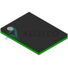
Surface mount 48-TFBGA package
Product Advantages
Fast access time suitable for high-speed applications
Stable and reliable storage solution
Wide temperature range for extreme environments
Key Technical Parameters
Memory Format SRAM - Asynchronous
Voltage Supply 2.7V ~ 3.6V
Operating Temperature -40°C ~ 85°C
Mounting Type Surface Mount
Package 48-TFBGA
Supplier Device Package 48-FBGA (7x7)
Quality and Safety Features
Robust static RAM technology
Built for industrial temperature ranges
Compatibility
General parallel interface for broad compatibility
Application Areas
Embedded systems
Communications equipment
Industrial control systems
Automotive electronics
Product Lifecycle
Active product status
Not nearing discontinuation
Several Key Reasons to Choose This Product
High-speed SRAM with quick access times for performance-critical applications
Reliable data retention over wide voltage and temperature ranges
Suitable for various industrial applications due to robust package and design
Infineon Technologies' reputation for high-quality and durable memory products

 CY62137EV30LL-45ZSXITInfineon TechnologiesIC SRAM 2MBIT PARALLEL 44TSOP II
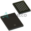 CY62137CV30LL-70BVXEInfineon TechnologiesIC SRAM 2MBIT PARALLEL 48VFBGA
 CY62137CVSL-7Cypress Semiconductor
 CY62137CV33LL-55BVICY


