

 MC9S08AC32MPUERNXP USA Inc.IC MCU 8BIT 32KB FLASH 64LQFP
 MC9S08AC32MFUENXP USA Inc.IC MCU 8BIT 32KB FLASH 64QFP
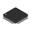 MC9S08AC32MPUEFreescale SemiconductorIC MCU 8BIT 32KB FLASH 64LQFP
 MC9S08AC32MFGEFreescale SemiconductorIC MCU 8BIT 32KB FLASH 44LQFP
 MC9S08AC48CFUEFreescale Semiconductor
 MC9S08AC48CFGER
- Emil***rperTech
- Jun 23, 2026
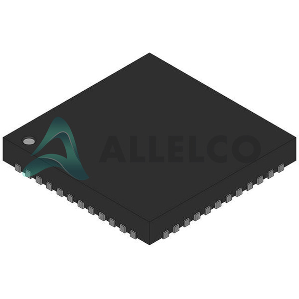
Image may be representation.
See specifications for product details.
See specifications for product details.
- EXPRESS OPTION
- Payment method
MC9S08AC48CFDE - Freescale Semiconductor
- Manufacturer Part Number
- MC9S08AC48CFDE
- Manufacturer
- Freescale Semiconductor, Inc. (NXP Semiconductors)
- Allelco Part Number
- 98D-MC9S08AC48CFDE
- Warranty
- 1 Year Allelco Warranty - Find out more
- Stock Status:
- 11,226 pcs available, New & Original
- Parts Description
- IC MCU 8BIT 48KB FLASH 48QFN
- Package
- 48-QFN-EP (7x7)
- Data sheet
- -
- RoHs Status
- Our certification
- In stock: 11226


