 S9S12P128J0MLHRNXP USA Inc.IC MCU 16BIT 128KB FLASH 64LQFP
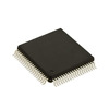 S9S12P128J0MQKNXP USA Inc.IC MCU 16BIT 128KB FLASH 80QFP
 S9S12P128JOMLHFreescale Semiconductor16-BIT MCU, S12 CORE, 128KB FLAS
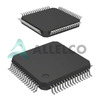 S9S12P128J0CLHFreescale SemiconductorIC MCU 16BIT 128KB FLASH 64LQFP
 S9S12P32J0CFTNXP Semiconductors
 S9S12P32J0CFTAnalog Devices Inc.16-bit MCU, S12 core, 32KB Flash
- Nath***rooks
- Jun 11, 2026
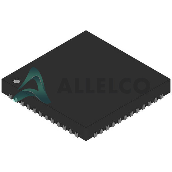
Image may be representation.
See specifications for product details.
See specifications for product details.
- EXPRESS OPTION
- Payment method
S9S12P128J0VFT - Freescale Semiconductor
- Manufacturer Part Number
- S9S12P128J0VFT
- Manufacturer
- Freescale Semiconductor, Inc. (NXP Semiconductors)
- Allelco Part Number
- 32D-S9S12P128J0VFT
- Warranty
- 1 Year Allelco Warranty - Find out more
- Stock Status:
- 14,980 pcs available, New & Original
- Parts Description
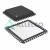
- IC MCU 16BIT 128KB FLASH 48QFN
- Package
- 48-QFN-EP (7x7)
- Data sheet
- -
- RoHs Status
- Our certification
- In stock: 14980


