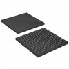

EP3C10F256C8 (1)
Manufacturer Part Number
EP3C10F256C8
Manufacturer
Intel
Introduction
Intel's Cyclone III series FPGA for embedded applications
Product Features and Performance
645 LABs/CLBs
10320 Logic Elements/Cells
423936 Total RAM Bits
182 Number of I/O
Supply Voltage Range of 1.15V to 1.25V
Surface Mount Technology
Operating Temperature Range 0°C to 85°C
Product Advantages
Optimized for low power consumption
High functionality with a large number of logic cells and memory
Robust I/O capabilities
Key Technical Parameters
645 LABs/CLBs
10320 Logic Elements/Cells
423936 Total RAM Bits
182 I/O Pins
15V to 1.25V Supply Voltage
0°C to 85°C Operating Temperature
Quality and Safety Features
Compliance with industry quality and safety standards
Reliable performance within the specified operating temperature range
Compatibility
Compatible with standard 256-LBGA integrated circuits
Application Areas
Suitable for automotive, industrial, medical, consumer electronics, and communication applications
Product Lifecycle
Active status
Not nearing discontinuation
Replacements and upgrades available
Several Key Reasons to Choose This Product
Advanced logic, memory, and I/O capabilities for complex applications
Low power consumption enhances system efficiency
Backed by Intel's reputation and support
Versatile use across multiple industries
Long-term availability and support for product integration
 EP3C10E144I7NIntelIC FPGA 94 I/O 144EQFP
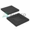 EP3C10M164C7NIntelIC FPGA 106 I/O 164MBGA
 EP3C10E144I7IntelIC FPGA 94 I/O 144EQFP
 EP3C10F256ALTERA


