View All

Please refer to the English Version as our Official Version.Return

Europe
France(Français) Germany(Deutsch) Italy(Italia) Russian(русский) Poland(polski) Czech(Čeština) Luxembourg(Lëtzebuergesch) Netherlands(Nederland) Iceland(íslenska) Hungarian(Magyarország) Spain(español) Portugal(Português) Turkey(Türk dili) Bulgaria(Български език) Ukraine(Україна) Greece(Ελλάδα) Israel(עִבְרִית) Sweden(Svenska) Finland(Svenska) Finland(Suomi) Romania(românesc) Moldova(românesc) Slovakia(Slovenská) Denmark(Dansk) Slovenia(Slovenija) Slovenia(Hrvatska) Croatia(Hrvatska) Serbia(Hrvatska) Montenegro(Hrvatska) Bosnia and Herzegovina(Hrvatska) Lithuania(lietuvių) Spain(Português) Switzerland(Deutsch) United Kingdom(English)
Asia/Pacific
Japan(日本語) Korea(한국의) Thailand(ภาษาไทย) Malaysia(Melayu) Singapore(Melayu) Vietnam(Tiếng Việt) Philippines(Pilipino)
Africa, India and Middle East
United Arab Emirates(العربية) Iran(فارسی) Tajikistan(فارسی) India(हिंदी) Madagascar(malaɡasʲ)
South America / Oceania
New Zealand(Maori) Brazil(Português) Angola(Português) Mozambique(Português)
North America
United States(English) Canada(English) Haiti(Ayiti) Mexico(español)
HomeProductsIntegrated Circuits (ICs)Embedded - FPGAs (Field Programmable Gate Array)EP4CGX150CF23C8N
EP4CGX150CF23C8N Image
Image may be representation.
See specifications for product details.
EXPRESS OPTION
Payment method

EP4CGX150CF23C8N - Intel

Manufacturer Part Number
EP4CGX150CF23C8N
Manufacturer
Intel
Allelco Part Number
32D-EP4CGX150CF23C8N
Warranty
1 Year Allelco Warranty - Find out more
Stock Status:
12,428 pcs available, New & Original
Parts Description
IC FPGA 270 I/O 484FBGA
Package
484-FBGA (23x23)
Data sheet
EP4CGX150CF23C8.pdf
RoHs Status
RoHS Compliant
Our certification
In stock: 12428
  • Unit Price: $149.20
  • Subtotal: $0.00

Want a better price?
Add to Cart and Submit RFQ now, we'll contact you immediately.

Quantity Unit Price Ext. Price
1+ $149.20 $149.20
200+ $57.74 $11,548.00
500+ $55.71 $27,855.00
1000+ $54.71 $54,710.00
The above prices does not include taxes and freight rates, which will be calculated on the order pages.

Specifications

EP4CGX150CF23C8N Tech Specifications
Intel - EP4CGX150CF23C8N technical specifications, attributes, parameters and parts with similar specifications to Intel - EP4CGX150CF23C8N

Product Attribute Attribute Value
Manufacturer Intel
Voltage - Supply 1.16V ~ 1.24V
Total RAM Bits 6635520
Supplier Device Package 484-FBGA (23x23)
Series Cyclone® IV GX
Package / Case 484-BGA
Package Tray
Product Attribute Attribute Value
Operating Temperature 0°C ~ 85°C (TJ)
Number of Logic Elements/Cells 149760
Number of LABs/CLBs 9360
Number of I/O 270
Mounting Type Surface Mount
Base Product Number EP4CGX150

Environmental & Export Classifications

ATTRIBUTE DESCRIPTION
RoHs Status RoHS Compliant
Moisture Sensitivity Level (MSL) 3 (168 Hours)
REACH Status REACH Unaffected
ECCN 3A991D
HTSUS 8542.39.0001

Parts Introduction

EP4CGX150CF23C8N Image
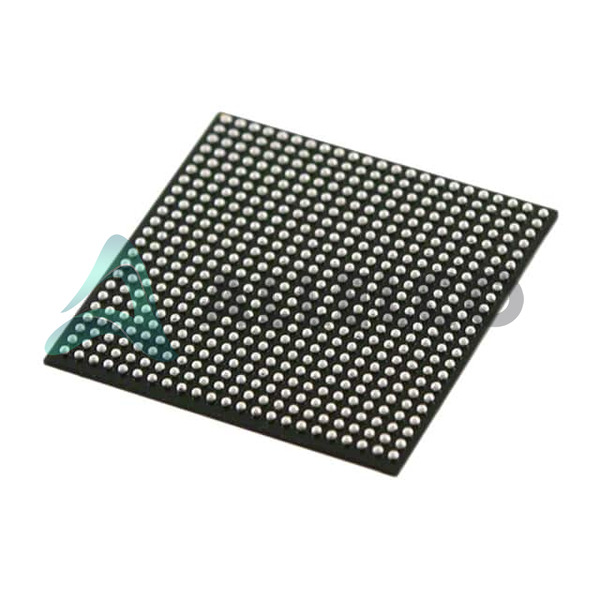
EP4CGX150CF23C8N (1)

Manufacturer Part Number

EP4CGX150CF23C8N

Manufacturer

Intel

Introduction

Intel Cyclone IV GX FPGA for embedded applications

Product Features and Performance

149760 logic elements

9360 LABs/CLBs

6635520 total RAM bits

270 I/O pins

16V to 1.24V supply voltage

Surface mount 484-BGA package

Product Advantages

High logic density for complex designs

Abundant memory for data-intensive operations

Flexible I/O interfacing

Low power consumption

Key Technical Parameters

Logic Elements/Cells: 149760

LABs/CLBs: 9360

RAM Bits: 6635520

I/O Number: 270

Voltage Supply Range: 1.16V ~ 1.24V

Operating Temperature Range: 0°C ~ 85°C

Quality and Safety Features

Extended operating temperature range for industrial applications

Robust BGA packaging for secure soldering

Compatibility

Standard voltage levels for interfacing

Compliant with multiple I/O standards

Application Areas

Industrial automation

Data processing

Telecommunications

Consumer electronics

Product Lifecycle

Active status

Continuous support from Intel

No near-term discontinuation, replacements, or upgrades announced

Several Key Reasons to Choose This Product

Intel reliability and support

Scalable solution for various applications

Adequate resources for high-performance tasks

Optimal balance between power consumption and computing power

Robust package suitable for different mounting needs

Frequently Asked Questions(FAQ)

How does the EP4CGX150CF23C8N handle dynamic power consumption under typical FPGA utilization scenarios?
The EP4CGX150CF23C8N, with its 149,760 logic elements and 6.6 Mbits of embedded memory, exhibits dynamic power that scales nonlinearly with toggle rates and resource utilization. At 50% logic utilization and 30% memory usage with a 100 MHz clock across multiple domains, typical dynamic power ranges from 1.8 W to 2.4 W when operating at 1.2 V core voltage. Designers should account for localized heating in high-activity regions, particularly around transceivers and high-fanout nets, which can increase junction temperature by 15–20°C above ambient even within the 0°C to 85°C operating range.
What are the implications of the 484-FBGA (23x23) package on PCB layout and thermal management for the EP4CGX150CF23C8N?
The 484-FBGA package with 0.8 mm ball pitch demands careful attention to via-in-pad design, solder mask definition, and impedance-controlled routing for high-speed I/O. Due to the high I/O count (270 pins) and dense ball grid, thermal vias beneath the package are essential to maintain junction temperature within limits. A minimum of 25–30 thermal vias connected to internal ground planes is recommended to achieve a thermal resistance (θJA) below 12°C/W in still air, especially when the device operates near maximum logic utilization.
How does the EP4CGX150CF23C8N compare to the EP4CE150F23C8N in terms of transceiver capability and power efficiency?
Unlike the EP4CE150F23C8N, which lacks integrated transceivers, the EP4CGX150CF23C8N includes three 3.125 Gbps transceivers optimized for PCIe Gen1 and CPRI applications. This integration reduces external PHY requirements but increases static power by approximately 300 mW. For designs requiring high-speed serial links, the GX variant offers a 20–30% reduction in total solution power compared to discrete transceiver implementations, despite higher FPGA core power.
What design considerations are necessary to meet timing closure with 149,760 logic elements in the EP4CGX150CF23C8N?
Achieving timing closure in the EP4CGX150CF23C8N requires hierarchical floorplanning due to the large logic capacity. With 9,360 LABs and long routing delays across the die, critical paths exceeding 200 ps of interconnect delay are common in flat designs. Using regional constraints and pipelining in high-fanout control logic can reduce setup violations by up to 40%. Additionally, enabling the Quartus Prime Physical Synthesis optimizations improves Fmax by 10–15% in complex state machines.
Can the EP4CGX150CF23C8N support simultaneous operation of multiple clock domains at frequencies above 200 MHz?
Yes, the EP4CGX150CF23C8N supports up to 16 independent clock domains using its global and regional clock networks. However, cross-domain interactions require careful metastability mitigation. When operating multiple domains above 200 MHz, skew between clock networks can reach 80–120 ps, necessitating synchronizer chains with at least two flip-flops for control signals. The device’s PLLs can generate phase-aligned clocks with jitter below 150 fs RMS, but board-level trace matching within ±5 mm is recommended for deterministic behavior.
How does the total RAM capacity of 6,635,520 bits in the EP4CGX150CF23C8N influence memory-intensive applications like packet buffering or DSP pipelines?
The 6.6 Mbit embedded memory in the EP4CGX150CF23C8N is distributed across M9K blocks, enabling efficient implementation of dual-port FIFOs and line buffers. For a 10 Gbps Ethernet application requiring 256 KB of jitter buffer, approximately 35% of the total memory is consumed, leaving sufficient margin for descriptor rings and statistics counters. However, memory access contention can reduce effective bandwidth by up to 25% when multiple logic blocks access shared M9K instances simultaneously, favoring partitioned memory architectures.
What are the reliability implications of operating the EP4CGX150CF23C8N at the upper end of its voltage supply range (1.24 V)?
Operating the EP4CGX150CF23C8N at 1.24 V increases static power by approximately 18% compared to 1.20 V and accelerates electromigration in long-term deployments. While within specification, sustained operation at maximum voltage and temperature (85°C junction) reduces mean time between failures (MTBF) by an estimated 30% over a 10-year lifecycle. For industrial applications, maintaining VCCINT at 1.18–1.20 V with active cooling extends reliability without sacrificing performance.
How does the I/O count of 270 pins in the EP4CGX150CF23C8N affect pin assignment strategy in high-speed interface designs?
With 270 I/O pins, the EP4CGX150CF23C8N allows flexible interface partitioning but requires strategic pin assignment to minimize crosstalk and impedance discontinuities. High-speed differential pairs (e.g., for LVDS or transceivers) should be placed in dedicated I/O banks with matched trace lengths (±2 mm) and adjacent ground pins. Assigning clock and control signals to centrally located I/O banks reduces skew and improves signal integrity, particularly when interfacing with DDR2/3 memory or high-pin-count ASICs.
What is the significance of the moisture sensitivity level (MSL 3) for the EP4CGX150CF23C8N in manufacturing workflows?
The EP4CGX150CF23C8N’s MSL 3 rating indicates a floor life of 168 hours after dry pack opening under ≤30°C and 60% RH. Exceeding this window increases the risk of popcorning during reflow, especially given the 484-FBGA package’s thickness and epoxy molding compound. Manufacturers must implement bake procedures (125°C for 24 hours) if the device is exposed beyond the limit, adding cost and delay. Proper handling protocols are essential for high-volume production lines.
How does the EP4CGX150CF23C8N perform in radiation-prone environments compared to non-GX Cyclone IV variants?
While not radiation-hardened, the EP4CGX150CF23C8N shows similar single-event upset (SEU) susceptibility to other Cyclone IV devices due to identical process technology. However, the integrated transceivers exhibit higher sensitivity to transient upsets in high-altitude or space-adjacent applications. For terrestrial use, triple modular redundancy (TMR) in critical state machines reduces SEU-induced failures by over 90%, but the GX transceivers require additional scrubbing logic not needed in non-GX counterparts.
What trade-offs exist when using the embedded transceivers in the EP4CGX150CF23C8N versus implementing high-speed serial links with external PHYs?
Using the built-in transceivers in the EP4CGX150CF23C8N reduces BOM complexity and board area by eliminating external PHYs, but limits flexibility in protocol support beyond 3.125 Gbps. External PHYs allow customization for protocols like SGMII or XAUI but introduce additional latency (2–4 ns per hop) and power (300–500 mW per channel). For applications requiring multiple serial links, the integrated solution in the EP4CGX150CF23C8N offers better power density and signal integrity when properly routed.
How should power sequencing be managed for the EP4CGX150CF23C8N in multi-rail systems?
The EP4CGX150CF23C8N requires core voltage (VCCINT) to be stable before or within 100 ms of I/O voltages (VCCIO). Reverse sequencing can cause latch-up in I/O buffers, particularly during hot-swap events. A typical power-on sequence involves ramping VCCINT to 1.2 V first, followed by VCCIO banks within 50 ms. Using voltage supervisors with adjustable thresholds ensures compliance, especially in systems with distributed power architectures where rail timing varies by ±20 ms.
What debugging challenges arise when prototyping with the 484-FBGA package of the EP4CGX150CF23C8N?
The 23x23 mm 484-FBGA package limits probe access, making traditional oscilloscope measurements difficult. Critical signals must be routed to test points or use embedded logic analyzers like SignalTap II. With 270 I/Os, signal integrity issues such as ground bounce or simultaneous switching noise (SSN) can mask functional errors. Designers should allocate 5–10% of I/Os for debug interfaces and use differential probing for high-speed nets to avoid loading effects.
How does the EP4CGX150CF23C8N support partial reconfiguration in real-world applications?
The EP4CGX150CF23C8N supports partial reconfiguration through the Quartus Prime software, allowing dynamic updates to specific logic regions while the rest of the design remains active. However, reconfiguration time for a 100 KLE module is approximately 8–12 ms, during which the affected logic is non-functional. This latency must be accounted for in real-time systems, and isolation logic is required to prevent glitches from propagating to stable regions during the update window.

Parts with Similar Specifications

The three parts on the right have similar specifications to Intel EP4CGX150CF23C8N

Product Attribute EP4CGX150CF23C7N EP4CGX150CF23C8 EP4CGX150CF23I7N EP4CGX150DF27C8N
Part Number EP4CGX150CF23C7N EP4CGX150CF23C8 EP4CGX150CF23I7N EP4CGX150DF27C8N
Manufacturer Intel Intel Intel Intel
Voltage - Supply - - - -
Supplier Device Package - 196-NFBGA (12x12) 16-PDIP 64-VQFN (9x9)
Mounting Type - Surface Mount Through Hole Surface Mount
Series - - - -
Base Product Number - DAC34H84 MAX500 ADS62P42
Total RAM Bits - - - -
Number of I/O - - - -
Number of LABs/CLBs - - - -
Number of Logic Elements/Cells - - - -
Package / Case - 196-LFBGA 16-DIP (0.300', 7.62mm) 64-VFQFN Exposed Pad
Package - Tape & Reel (TR) Tube Tape & Reel (TR)
Operating Temperature - -40°C ~ 85°C 0°C ~ 70°C -40°C ~ 85°C

EP4CGX150CF23C8N Datasheet PDF

Download EP4CGX150CF23C8N pdf datasheets and Intel documentation for EP4CGX150CF23C8N - Intel.

Datasheets
Cyclone IV Device Datasheet.pdf Cyclone IV Device Handbook.pdf Virtual JTAG Megafuntion Guide.pdf
Errata
2.73KHz.pdf

Customer Reviews

Evaluation: 10 Articles

  • Nath***rooks
    Jun 11, 2026

    Installed this power component in a converter board. Output remained stable under different load conditions and thermal performance was better than expected.

  • Dani***alkerTech
    Jun 1, 2026

    Product works, but setup took more effort than expected. Once configured the MCU ran reliably, although documentation support felt older compared with newer platforms. Fine for maintenance projects.

  • Yuki***aka88
    May 26, 2026

    信号通信プロジェクトでこのRS-485トランシーバーを使用しました。設置は簡単で、長距離ケーブルでも通信は安定していました。消費電力も、以前使用していたものより低くなっています。

  • Stev***aker
    May 20, 2026

    Solid diode for power rectification. Works well in switching circuits.

  • Bran***Lewis
    May 11, 2026

    Compact FPGA with good performance. Suitable for basic signal processing tasks.

  • Oliv***arris
    May 7, 2026

    Reliable I/O expander. Works well in embedded control applications.

  • Jess***Jones
    Apr 17, 2026

    It offers good value for the price, and the specifications match the description. I’ve been using it for two days with no issues, and I’ll definitely buy it again if I need it in the future.

  • Mich***Smith
    Apr 17, 2026

    Shipping was on time, the component pins are neatly aligned, and I tested 10 of them with a multimeter—all readings were within the specified range. Highly recommended.

  • Aman***arris
    Apr 3, 2026

    It was great—the entire process, from placing the order to receiving the package, went very smoothly. The components were consistent, the price was fair, and I had a very pleasant shopping experience.

  • Mike***nch
    Apr 3, 2026

    Better than expected! The resistance and capacitance readings were spot-on, and it passed the test on the first try. The service was reliable, and the packaging was thoughtful—I highly recommend it.

Write a Review

Your Email address will not be published.

Shipment

Delivery Time

In-stock items can be shipped within 24 hours. Some parts will be arranged for delivery within 1-2 days from the date all items arrive at our warehouse. And Allelco ships order once a day at about 17:00, except Sunday. Once the goods are shipped, the estimated delivery time depends on the shipping methods and Delivery destination. The table below shows are the logistic time for some common countries.

Delivery Cost

  1. Use your express account for shipment if you have one.
  2. Use our account for the shipment. Refer to the table below for the approximate charges.
(Different time frame / countries / package size has different price.)

Delivery Method

  1. Global Common Shipment by DHL / UPS / FedEx / TNT / EMS / SF we support.
  2. Others more shipping ways, please get in touch with your customer manager.

Common Countries Logistic Time Reference
Region Country Logistic Time(Day)
America United States 5
Brazil 7
Europe Germany 5
United Kingdom 4
Italy 5
Oceania Australia 6
New Zealand 5
Asia India 4
Japan 4
Middle East Israel 6
DHL & FedEx Shipment Charges Reference
Shipment charges(KG) Reference DHL(USD$)
0.00kg-1.00kg USD$30.00 - USD$60.00
1.00kg-2.00kg USD$40.00 - USD$80.00
2.00kg-3.00kg USD$50.00 - USD$100.00
Note:
The above table is for reference only. There may have some data bias for the uncontrollable factors.
Contact us if you have any questions.
  • QC (Quality Warranty)
  • Payment Support
  • Packaging
  • Certifications & Memberships

QC (Quality Warranty)

Allelco is committed to exceeding customer expectations through customer service excellence, order accuracy, and on-time delivery.
This is achieved through our commitment to the continual improvement of our processes, services, and products.


Strict quality inspection builds a solid foundation for electronic component quality.
  1. Visual inspection
  2. Performance testing and reliability verification
  3. Standardized full-process testing
  4. Precise control of every parameter
We eliminate defective components and ensure the stable operation of electronic devices through professional quality standards.

Payment Support

The payment method can be chosen from the methods shown below: Wire Transfer (T/T, Bank Transfer), Western Union, Credit card, PayPal.
  • HKBea
  • Paypal
  • MasterCard
  • Western-Union
  • VISA
Stable Delivery, Sincere Partnership — Your Faithful Supply Chain Partner
  • Efficient Supply Management
  • Cost-Saving Procurement
  • Fast Sourcing & Delivery
Contact us if you have any questions.

Packaging

Electrostatic Discharge Protection and Handling

All electrostatic-sensitive components are handled in accordance with electrostatic discharge control procedures. The products are hermetically sealed in anti-static safe packaging to prevent electrostatic damage. Appropriate labeling is also applied for identification and traceability. This ensures product integrity during storage, handling and transportation.


ESD

Certifications & Memberships

Third-party certified, strict quality control. Our certification
  • ISO 9001: 2015
  • ISO 13485: 2016
  • ISO 14001: 2015
  • ISO 28000: 2007
  • ISO 45001: 2018
  • GB/T 27922-2011
  • SMTA
  • IPC
  • ESD
  • PSMA
EP4CGX150CF23C8N Image

EP4CGX150CF23C8N

Intel
32D-EP4CGX150CF23C8N

Want a better price? Add to Cart and Submit RFQ now, we'll contact you immediately.

0 RFQ
Shopping cart (0 Items)
It is empty.
Compare List (0 Items)
It is empty.
Feedback

Your feedback matters! At Allelco, we value the user experience and strive to improve it constantly.
Please share your comments with us via our feedback form, and we'll respond promptly.
Thank you for choosing Allelco.

Subject
E-mail
Comments
Captcha
Drag or click to upload file
Upload File
types: .xls, .xlsx, .doc, .docx, .jpg, .png and .pdf.
Max file size: 10MB