
LC4256ZE-7TN100C (1)
Manufacturer Part Number
LC4256ZE-7TN100C
Manufacturer
Lattice Semiconductor
Introduction
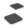
The LC4256ZE-7TN100C is a high-performance, in-system programmable Complex Programmable Logic Device (CPLD) from Lattice Semiconductor's ispMACH® 4000ZE series, housed in a 100-LQFP package.
Product Features and Performance
In-system Programmable
Supports 256 macrocells and 16 logic blocks
64 available I/O pins
Operating temperature range from 0°C to 90°C
Maximum delay time of 7.5 ns
Low voltage supply range from 1.7V to 1.9V
Product Advantages
High integration of logic elements reduces overall system cost
Low power consumption enhancing device longevity and reliability under varying environmental conditions
Key Technical Parameters
Number of Logic Elements/Blocks: 16
Number of Macrocells: 256
Number of I/O: 64
Voltage Supply - Internal: 1.7V ~ 1.9V
Delay Time tpd(1) Max: 7.5 ns
Quality and Safety Features
Robust surface mount package (100-LQFP)
Operates reliably within an industrial temperature range of 0°C to 90°C
Compatibility
Compatible with surface mount technology for ease of assembly on printed circuit boards
Application Areas
Ideal for automotive, telecommunications, data processing, industrial controls, and security systems
Product Lifecycle
Currently active with ongoing manufacturer support
Future replacement or upgrade options available
Several Key Reasons to Choose This Product
Low power operation and in-system programmability offer flexibility and extended product life
High I/O pin count and macrocell count allow for versatile and complex logic design capabilities
Supported by Lattice design and development tools ensuring ease of integration and implementation
Optimal for high-performance industrial applications due to robust temperature and voltage specifications
Trusted manufacturer with a strong reputation in CPLD products
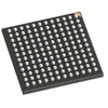

 LC4384B-10F256ILattice Semiconductor CorporationIC CPLD 384MC 10NS 256FPBGA
 LC4256ZE-P-EVNLattice Semiconductor CorporationBOARD EVAL ISPMACH 4256ZE
 LC4256ZE-B-EVNLattice Semiconductor CorporationBOARD BREAKOUT ISPMACH 4256ZE
 LC4256ZE-5MN144CLattice Semiconductor CorporationIC CPLD 256MC 5.8NS 144CSBGA
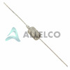 LC43/TRMicrochip TechnologyTVS DIODE 43VWM 76.7VC DO202AA
 LC43Microchip TechnologyTVS DIODE 43VWM 76.7VC DO202AA
 LC4256ZE-5TN100C-7ILattice Semiconductor


