
LCMXO2-1200HC-6TG100I (1)
Manufacturer Part Number
LCMXO2-1200HC-6TG100I
Manufacturer
Lattice Semiconductor
Introduction
High-performance, low-power FPGA for embedded applications
Part of the MachXO2 series
Product Features and Performance
1280 logic elements
65,536 total RAM bits
160 LABs/CLBs
High-speed FPGA fabric
Flexible I/O with 79 user I/Os
Product Advantages
Low power consumption
Reprogrammable and reconfigurable
Ideal for embedded applications
Key Technical Parameters
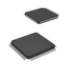
100-TQFP (14x14) package
Surface mount
Operating temperature: -40°C to 100°C
Supply voltage: 2.375V to 3.465V
Quality and Safety Features
RoHS3 compliant
Compatibility
Compatible with the MachXO2 series
Application Areas
Embedded systems
Industrial automation
Home appliances
Consumer electronics
Product Lifecycle
Current product, no discontinuation planned
Upgrades and replacements available within the MachXO2 series
Key Reasons to Choose This Product
High-performance FPGA for embedded applications
Low power consumption
Reprogrammable and reconfigurable
Ideal for a wide range of embedded systems
 LCMXO2-1200HC-6MG132CLattice Semiconductor CorporationIC FPGA 104 I/O 132CSBGA
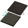 LCMXO2-1200UHC-4FTG256CLattice Semiconductor CorporationIC FPGA 206 I/O 256FTBGA
 LCMXO2-1200HC-6SG32CLattice


