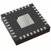

ADS1148IRHBT (1)
Manufacturer Part Number
ADS1148IRHBT
Manufacturer
Texas Instruments
Introduction
ADS1148IRHBT is a high-performance 16-bit Analog to Digital Converter (ADC) suited for advanced data acquisition in scientific and industrial applications.
Product Features and Performance
16-bit resolution providing high accuracy
Sampling rate of 2kSPS
Configurable as 4 differential or 7 single-ended inputs
Integrated multiplexer (MUX), programmable gain amplifier (PGA), and ADC
Communication via SPI interface
Supports both external and internal references
Sigma-Delta architecture enhancing noise performance
Operating temperature range from -40°C to 105°C
Product Advantages
Precision data acquisition with high-resolution ADC
Flexible input configuration adapting to various signal types
Integrated features reduce need for external components
Robust operation in extreme temperatures
Key Technical Parameters
Number of Bits: 16
Sampling Rate: 2k per second
Number of Inputs: 4 differential, 7 single-ended
Voltage Supply, Analog: 2.7V to 5.25V
Voltage Supply, Digital: 2.7V to 5.25V
Quality and Safety Features
Extended operating temperature range ensures reliable performance under extreme conditions
Sigma-Delta architecture minimizes signal noise and enhances accuracy
Compatibility
SPI communication interface ensures compatibility with a broad range of microcontrollers and digital systems
Application Areas
Scientific research instrumentation
Industrial control systems
Medical equipment monitoring
Product Lifecycle
Product status: Active
Not close to discontinuation; replacements and upgrades available
Several Key Reasons to Choose This Product
High accuracy and resolution suitable for precision applications
Flexible input and reference options accommodate diverse use cases
Integrated PGA, MUX, and ADC simplify system design
Wide operating temperature range ensures reliability in challenging environments
SPI interface compatibility with various digital control systems


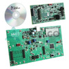 ADS1147EVM-PDKTexas InstrumentsKIT PERFORMANCE DEMO FOR ADS1147
 ADS1147EVMTexas InstrumentsEVAL MODULE FOR ADS1147
 ADS1147IPWRTexas InstrumentsIC ADC 16BIT SIGMA-DELTA 20TSSOP
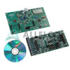 ADS1148EVM-PDKTexas InstrumentsKIT PERFORMANCE DEMO FOR ADS1148
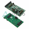 ADS1148EVMTexas InstrumentsEVAL MODULE FOR ADS1148
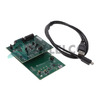 ADS1148V2EVM-PDKTexas InstrumentsEVAL BOARD FOR ADS1148
 ADS1147IPWTexas Instruments


