ADS58H43IZCR (1)
Manufacturer Part Number
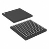
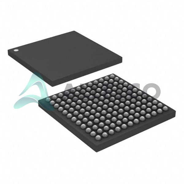
ADS58H43IZCR
Manufacturer
Texas Instruments
Introduction
High-performance 14-bit ADC supporting simultaneous sampling at 250 MSPS
Product Features and Performance
14-bit resolution
Dual ADC channels for simultaneous sampling
250 MSPS sampling rate
Four differential inputs
Pipelined architecture with internal reference
LVDS parallel data interface
Sample/Hold functionality
Supports wide range of supply voltages
Product Advantages
Simultaneous sampling for accurate multi-channel measurement
High sampling rate suitable for high-speed applications
Low-power consumption enhancing system efficiency
Built-in features to ease system design and integration
Key Technical Parameters
Number of Bits: 14
Sampling Rate: 250M samples per second
Number of Inputs: 4
Input Type: Differential
Architecture: Pipelined
Voltage - Supply, Analog: 1.8V to 2V, 3.15V to 3.45V
Voltage - Supply, Digital: 1.7V to 2V
Operating Temperature: -40°C to 85°C
Quality and Safety Features
Robust LFBGA package for reliable operation
Extended operating temperature range
Precision data conversion improves system accuracy
Compatibility
Compatible with various microprocessors via LVDS interface
Meets the requirements for diverse digital systems
Application Areas
Medical imaging
Data acquisition systems
Wireless infrastructure
Test and measurement equipment
Product Lifecycle
Active status product
Continued manufacturer support and availability
Several Key Reasons to Choose This Product
Texas Instruments' reputation for quality and reliability
High-speed, high-resolution ADC capabilities
Simultaneous multi-channel data acquisition
Suitable for mission-critical applications requiring precision
Supports advanced digital signal processing needs
Ease of design and integration into existing systems
Ongoing product support and longevity in the market

 ADS58C48IPFPRTexas InstrumentsIC ADC 11BIT 200M 80HTQFP
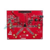 ADS58H40EVMTexas InstrumentsEVAL MODULE FOR ADS58H40
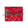 ADS58H43EVMTexas InstrumentsMODULE EVAL FOR ADS58H43
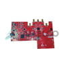 ADS58J64EVMTexas InstrumentsEVAL BOARD FOR ADS58J64
 ADS58C48IPFPTexas InstrumentsIC ADC 11BIT 200M 80HTQFP
 ADS58C48EVMTexas InstrumentsEVAL MODULE FOR ADS58C48
 ADS58J63EVMTexas InstrumentsEVAL MODULE ADS58J63
 ADS58J63IRMPRTexas InstrumentsIC RECEIVER 14BIT 500M 72VQFN


