
Manufacturer Part Number
ADS7960QDBTRQ1
Manufacturer
Texas Instruments
Introduction
High-speed, multichannel, automotive-grade, 8-bit analog-to-digital converter
Product Features and Performance
8-bit resolution
1M samples per second sampling rate
12 single-ended input channels
SPI data interface
MUX-PGA-S/H-ADC configuration
Single SAR A/D converter
Programmable gain amplifier (PGA) feature
External reference type
Operates on 2.7V to 5.25V analog supply voltage
Operates on 1.7V to 5.25V digital supply voltage
Operating temperature range from -40°C to 125°C
Product Advantages
Optimized for automotive applications
AEC-Q100 qualified
High-speed data acquisition
Multiplexed input channels for monitoring multiple signals
Built-in PGA for signal conditioning
SAR architecture for low-power and high-throughput
Wide range of supply voltages for flexible power management
Key Technical Parameters
Number of Bits: 8
Sampling Rate: 1MSPS
Number of Inputs: 12
Input Type: Single Ended
Data Interface: SPI
Architecture: SAR
Voltage Supply, Analog: 2.7V to 5.25V
Voltage Supply, Digital: 1.7V to 5.25V
Operating Temperature: -40°C to 125°C
Quality and Safety Features
AEC-Q100 automotive qualification
Robust temperature performance
Suitable for safety-critical applications
Compatibility
Compatible with SPI protocol interfaces
Flexible voltage compatibility for mixed-voltage systems
Application Areas
Automotive electronics
Data acquisition systems
Sensor monitoring
Industrial control systems
Product Lifecycle
Active product status
Not nearing discontinuation
Availability of replacements or upgrades is ensured by manufacturer
Several Key Reasons to Choose This Product
Robust design suitable for harsh automotive environments
High-speed ADC enabling precise and rapid signal conversion
Multichannel input for comprehensive system monitoring
Integrated features, such as PGA for signal amplification, reducing additional component count
Texas Instruments' reputation for quality and reliability in semiconductor manufacturing
Long product lifecycle with continued manufacturer support
Surface mount design for modern, compact PCB layouts

 ADS7960SRHBTTexas InstrumentsIC ADC 8BIT SAR 32VQFN
 ADS7958SRGERTexas InstrumentsIC ADC 8BIT SAR 24VQFN
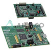 ADS7961EVM-PDKTexas InstrumentsKIT PERFORMANCE DEMO FOR ADS7961


