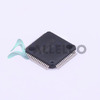
View All

Please refer to the English Version as our Official Version.Return

Europe
France(Français) Germany(Deutsch) Italy(Italia) Russian(русский) Poland(polski) Czech(Čeština) Luxembourg(Lëtzebuergesch) Netherlands(Nederland) Iceland(íslenska) Hungarian(Magyarország) Spain(español) Portugal(Português) Turkey(Türk dili) Bulgaria(Български език) Ukraine(Україна) Greece(Ελλάδα) Israel(עִבְרִית) Sweden(Svenska) Finland(Svenska) Finland(Suomi) Romania(românesc) Moldova(românesc) Slovakia(Slovenská) Denmark(Dansk) Slovenia(Slovenija) Slovenia(Hrvatska) Croatia(Hrvatska) Serbia(Hrvatska) Montenegro(Hrvatska) Bosnia and Herzegovina(Hrvatska) Lithuania(lietuvių) Spain(Português) Switzerland(Deutsch) United Kingdom(English)
Asia/Pacific
Japan(日本語) Korea(한국의) Thailand(ภาษาไทย) Malaysia(Melayu) Singapore(Melayu) Vietnam(Tiếng Việt) Philippines(Pilipino)
Africa, India and Middle East
United Arab Emirates(العربية) Iran(فارسی) Tajikistan(فارسی) India(हिंदी) Madagascar(malaɡasʲ)
South America / Oceania
New Zealand(Maori) Brazil(Português) Angola(Português) Mozambique(Português)
North America
United States(English) Canada(English) Haiti(Ayiti) Mexico(español)
HomeProductsIntegrated Circuits (ICs)Data Acquisition - Analog to Digital Converters (ADC)ADS8568SRGCR
ADS8568SRGCR Image
Image may be representation.
See specifications for product details.
EXPRESS OPTION
Payment method

ADS8568SRGCR - Texas Instruments

Manufacturer Part Number
ADS8568SRGCR
Manufacturer
Texas Instruments
Allelco Part Number
32D-ADS8568SRGCR
Warranty
1 Year Allelco Warranty - Find out more
Stock Status:
2,026 pcs available, New & Original
Parts Description
IC ADC 16BIT SAR 64VQFN
Package
64-VQFN (9x9)
Data sheet
ADS8568SRGCR.pdf

HTML Datasheet

ADS8528,48,68.pdf
RoHs Status
ROHS3 Compliant
Our certification
In stock: 2026
  • Unit Price: $13.09
  • Subtotal: $0.00

Want a better price?
Add to Cart and Submit RFQ now, we'll contact you immediately.

Quantity Unit Price Ext. Price
1+ $13.09 $13.09
10+ $12.56 $125.60
30+ $11.64 $349.20
100+ $10.84 $1,084.00
The above prices does not include taxes and freight rates, which will be calculated on the order pages.

Specifications

ADS8568SRGCR Tech Specifications
Texas Instruments - ADS8568SRGCR technical specifications, attributes, parameters and parts with similar specifications to Texas Instruments - ADS8568SRGCR

Product Attribute Attribute Value
Manufacturer Texas Instruments
Voltage - Supply, Digital 2.7V ~ 5.5V
Voltage - Supply, Analog 5V
Supplier Device Package 64-VQFN (9x9)
Series -
Sampling Rate (Per Second) 500k
Reference Type External, Internal
Ratio - S/H:ADC 1:1
Package / Case 64-VFQFN Exposed Pad
Package Tape & Reel (TR)
Operating Temperature -40°C ~ 125°C
Product Attribute Attribute Value
Number of Inputs 8
Number of Bits 16
Number of A/D Converters 1
Mounting Type Surface Mount
Input Type Single Ended
Features Simultaneous Sampling
Data Interface SPI, Parallel
Configuration S/H-ADC
Base Product Number ADS8568
Architecture SAR

Environmental & Export Classifications

ATTRIBUTE DESCRIPTION
RoHs Status ROHS3 Compliant
Moisture Sensitivity Level (MSL) 3 (168 Hours)
REACH Status REACH Unaffected
ECCN EAR99
HTSUS 8542.39.0001

Parts Introduction

ADS8568SRGCR Image
ADS8568SRGCR (1)

Manufacturer Part Number

ADS8568SRGCR

Manufacturer

Texas Instruments

Introduction

The ADS8568SRGCR is a high-performance, 16-bit Analog to Digital Converter (ADC) from Texas Instruments, designed for precision data acquisition in applications requiring high-speed simultaneous sampling.

Product Features and Performance

16-bit resolution provides high accuracy in measurement

Sampling Rate of 500k samples per second allows for high-speed data acquisition

8 Single Ended inputs enable multi-channel signal acquisition

SPI and Parallel data interfaces offer flexibility in system design

Simultaneous Sampling feature ensures accurate multi-channel measurements

Sar Architecture ensures consistent and reliable conversion results

Supports both External and Internal reference types for versatility in applications

Operates with Analog Supply Voltage of 5V and Digital Supply Voltage of 2.7V to 5.5V

Product Advantages

High resolution and sampling rate improve measurement precision and speed

Multiple input channels allow for comprehensive data collection without additional components

Flexible interface options make integration into various systems easy

Robust temperature range (-40°C to 125°C) suits a wide range of environments

Key Technical Parameters

Number of Bits: 16

Sampling Rate (Per Second): 500k

Number of Inputs: 8

Input Type: Single Ended

Data Interface: SPI, Parallel

Architecture: SAR

Operating Temperature: -40°C to 125°C

Voltage Supply, Analog: 5V

Voltage Supply, Digital: 2.7V to 5.5V

Quality and Safety Features

Manufactured by Texas Instruments, ensuring high quality and reliability

Rated for operation in harsh environments (-40°C to 125°C)

Compatibility

Interface compatibility with SPI and Parallel systems for easy integration

Flexible voltage supply range supports a variety of power systems

Application Areas

Industrial process control

Medical instrumentation

Data acquisition systems

Automotive systems

Communication equipment

Product Lifecycle

Product Status: Active

Continual support and production ensure long-term availability

No immediate discontinuation, with potential future upgrades or replacements

Several Key Reasons to Choose This Product

High-performance 16-bit ADC with fast sampling rate for precise data acquisition

Multi-channel input and simultaneous sampling features cater to advanced application needs

Flexible interfacing and power supply options facilitate easy system integration

Dependable quality and support from Texas Instruments

Suitable for a wide range of applications due to robust operating temperature range and multi-channel capabilities

Frequently Asked Questions(FAQ)

How does the ADS8568SRGCR handle simultaneous sampling across its eight input channels, and what impact does this have on signal integrity in multi-sensor industrial monitoring systems?
The ADS8568SRGCR supports simultaneous sampling, meaning all eight input channels capture data at exactly the same instant, even though each channel is processed sequentially by the SAR ADC. This architectural feature is critical for applications like current sensing in motor drives or vibration analysis in rotating machinery, where phase alignment between signals must be preserved. Without simultaneous sampling, time delays between channels could introduce measurement errors in dynamic conditions. In practice, this means that when using all eight inputs at full speed (500 kSPS per channel), the total throughput remains 500 kSPS, but each channel effectively delivers samples spaced 2 μs apart with perfect temporal correlation.
What are the power consumption trade-offs when operating the ADS8568SRGCR in low-power mode versus full-speed continuous conversion, and how should these influence system-level design for battery-powered data loggers?
The ADS8568SRGCR consumes approximately 3.2 mW at 500 kSPS with a 5V analog supply, but can reduce power to under 1 mW when idle or using shutdown modes. However, transitioning from sleep to active mode requires a startup delay of about 20 μs during which no conversions occur. For battery-operated devices logging sensor data every few seconds, this delay may be acceptable, but for high-resolution event-based recording, the average power savings may not justify the latency penalty. Engineers must model duty cycle efficiency carefully—for example, a device waking every 100 ms would spend over 99% of time in low-power state, making the ADS8568SRGCR viable only if wake-up overhead doesn’t dominate energy budget.
Can the ADS8568SRGCR be used with a 3.3V logic supply while maintaining compatibility with modern microcontrollers, and what interface considerations arise?
Yes, the digital interface of the ADS8568SRGCR operates from 2.7V to 5.5V, allowing direct connection to 3.3V microcontrollers such as MSP430 or ARM Cortex-M series without level shifting. The SPI and parallel interfaces are fully compatible with 3.3V CMOS levels, provided the analog supply remains within specification. However, care must be taken during PCB layout to isolate digital return currents from analog ground paths to avoid introducing noise through shared impedance. Many designers tie both AVdd and DVdd to the same clean 3.3V rail, decoupling them locally with separate capacitors near the IC to maintain stability.
How does the effective number of bits (ENOB) degrade under typical noise conditions when using an external reference versus the internal reference on the ADS8568SRGCR?
With a stable 2.5V external reference, the ADS8568SRGCR achieves an ENOB of around 14.5 bits under laboratory conditions. However, when using the internal bandgap reference, temperature drift and long-term stability limit ENOB to approximately 13.8 bits over the industrial temperature range. In noisy environments—such as those near switching regulators—the differential nonlinearity (DNL) may approach ±1 LSB, reducing linearity and thus ENOB further. Therefore, precision applications requiring better than 14-bit performance should prioritize an external, low-noise voltage reference, especially when operating near the extremes of the -40°C to 125°C range.
What is the maximum allowable input signal amplitude for each channel of the ADS8568SRGCR, and how does this constrain sensor interface design?
Each input accepts unipolar signals up to Vref (typically 2.5V) with respect to AGND, giving a full-scale range of approximately 5V peak-to-peak when referenced to ground. Exceeding Vref causes immediate saturation, while inputs below AGND risk damaging the ESD protection diodes unless clamped externally. For sensors outputting millivolt-level signals (e.g., strain gauges or thermocouples), an instrumentation amplifier with gain >100 is usually required before routing to the ADS8568SRGCR. Improper scaling can lead to quantization loss, reducing effective resolution by multiple bits.
How does the aperture jitter specification affect timing accuracy in fast transient capture scenarios using the ADS8568SRGCR?
Although not explicitly detailed in the datasheet, SAR ADCs like the ADS8568SRGCR do not suffer from aperture jitter in the same way as sample-and-hold based converters. Instead, their conversion timing is deterministic and governed by clock stability. At 500 kSPS, a 1 LSB error corresponds to about 1.5 μs, so clock jitter must remain well below this threshold to preserve linearity. Using a crystal oscillator with phase noise < -100 dBc/Hz at 1 kHz offset ensures minimal degradation. In contrast, integrating over multiple samples averages out random jitter effects, making the ADS8568SRGCR suitable for statistical measurements rather than ultra-precise single-shot timing.
When comparing the ADS8568SRGCR to the ADS8361, which offers higher sampling rate but fewer channels, what key factors should guide the choice for a distributed sensor network?
The ADS8568SRGCR provides eight channels at 500 kSPS per channel, whereas the ADS8361 offers 250 kSPS on four channels. While raw bandwidth favors the ADS8568SRGCR, the ADS8361 consumes significantly less power and has a smaller footprint. For a distributed network where each node handles only one or two sensors, the lower throughput of the ADS8361 may suffice, allowing simpler filtering and reduced post-processing load. Conversely, centralized monitoring requiring synchronized multi-axis data acquisition benefits more from the ADS8568SRGCR’s simultaneous sampling and higher channel count, despite slightly higher quiescent current.
How does the 64-VQFN package thermal performance compare to larger packages for sustained high-speed operation of the ADS8568SRGCR?
The 64-VQFN (9x9 mm) package has limited exposed pad conduction compared to packages with larger thermal pads or metal bases. Under continuous 500 kSPS operation with all channels active, junction temperature can rise 20–30°C above ambient in poorly laid-out boards due to poor heat spreading through the PCB. Proper implementation includes a solid ground plane beneath the IC, multiple vias connecting the exposed pad to an inner layer, and avoiding copper pours directly adjacent to sensitive analog traces. Thermal resistance is typically 35–40°C/W, necessitating attention to layout for reliable operation near 125°C ambient.
What are the recommended decoupling strategies for minimizing digital switching noise coupling into the analog domain of the ADS8568SRGCR?
Separate analog and digital power domains are strongly advised, with AVdd and DVdd connected at a single point near the IC using a ferrite bead or 0Ω resistor. Each supply should have a dedicated 10μF tantalum capacitor in parallel with a 0.1μF ceramic capacitor placed within 3 mm of the pins. Additionally, guard rings around analog inputs and careful routing of digital lines away from input traces prevent capacitive coupling. Clock signals should be routed on inner layers shielded by ground planes to minimize radiated interference that could manifest as spurious codes in high-resolution measurements.
Is it feasible to daisy-chain multiple ADS8568SRGCR devices over SPI for expanding channel counts beyond eight, and what limitations apply?
Yes, the serial interface supports daisy-chaining via the SDI pin, allowing multiple ADCs to share one SPI bus. However, each device requires individual chip-select lines or a shift register to manage selection. Critical constraints include cumulative propagation delay across chains (typically 15–20 ns per stage) and increased susceptibility to noise due to longer trace lengths. Moreover, simultaneous sampling cannot be extended across chips without external synchronization, defeating one of the ADS8568SRGCR’s key advantages. Thus, while possible, this approach is only beneficial when adding non-synchronized channels or when space constraints demand compact stacking.
How does the integral nonlinearity (INL) specification of the ADS8568SRGCR impact calibration requirements in precision weigh-scale applications?
The ADS8568SRGCR specifies INL of ±2 LSB typical, which translates to less than 0.003% FS error. For high-end scales requiring <0.01% accuracy, this margin may be sufficient without calibration, but consumer-grade systems might need software correction tables. The monotonicity guarantee ensures no missing codes across the entire range, simplifying linearization algorithms. However, temperature-induced drift in the ADC core can shift INL characteristics over time, so periodic recalibration or use of an internal diagnostic mode may be necessary in unattended installations.
What precautions are essential when handling the ADS8568SRGCR during prototyping to prevent electrostatic discharge damage?
As a CMOS device with Moisture Sensitivity Level 3, the ADS8568SRGCR requires standard ESD precautions: working on grounded surfaces, using wrist straps, and storing in conductive foam or antistatic bags. During soldering, hot-air rework stations should limit airflow temperature to <300°C and duration to <10 seconds to avoid bond-wire lift-off. The human body model (HBM) rating is typically Class 2, meaning moderate sensitivity; thus, improper handling risks latent failures manifesting later under thermal stress. Always follow IPC-JEDEC J-STD-020 guidelines during assembly.
How does the sampling rate interact with anti-aliasing filter design when using the ADS8568SRGCR in audio or vibration analysis?
At 500 kSPS, the Nyquist frequency is 250 kHz, so anti-aliasing filters must attenuate frequencies above this sharply. A fourth-order sinc filter with cutoff at 200 kHz provides adequate roll-off, but phase distortion may affect time-domain analysis. Alternatively, programmable decimation can reduce effective sample rate after initial high-rate capture, relaxing filter requirements. For vibration monitoring up to 10 kHz, a simple RC low-pass with fc = 30 kHz suffices, yielding >60 dB attenuation at Nyquist. Oversampling by 10× improves SNR by ~15 dB, enhancing dynamic range without increasing ADC complexity.
Can the ADS8568SRGCR operate reliably in automotive environments subject to ISO 16750 transients, and what additional protections are needed?
The ADS8568SRGCR itself meets industrial temperature ranges (-40°C to 125°C), but automotive compliance requires external protection. Inputs should be clamped using TVS diodes rated for ISO 7637 pulses, and power supplies isolated via bidirectional transient suppressors. Layout must ensure creepage distances meet automotive safety standards, and ground planes segmented to prevent fault propagation. Without such measures, even minor voltage spikes can latch internal nodes or corrupt registers, leading to unpredictable behavior in safety-critical systems.
How does the reference buffer requirement differ between internal and external references when driving the ADS8568SRGCR’s analog inputs?
When using an external reference, the REF+ pin drives a high-impedance node, requiring a unity-gain buffer with low output impedance (<1 Ω) and high PSRR to maintain accuracy. The internal reference also benefits from buffering, but its source impedance is lower. Poor buffering introduces droop during conversion bursts, degrading linearity. In practice, op-amps like OPA188 or LM4040 with bypass capacitors close to the REF pins ensure stable reference delivery, particularly important when sharing the reference among multiple precision circuits.
What role does the hold capacitor settling time play in achieving full 16-bit accuracy with the ADS8568SRGCR?
The sample-and-hold architecture uses a switched-capacitor network whose settling time determines how quickly the input tracks the signal before conversion begins. At 500 kSPS, the tracking period is 1 μs, which must accommodate both acquisition and conversion phases. Full 16-bit accuracy demands settling within 0.5 LSB (~15 μV for 5V FS), achievable only if the source impedance is <1 kΩ and the input signal changes slowly relative to the sample interval. High-frequency components or large step inputs may cause residual charge errors, necessitating either oversampling or pre-filtering.
How does the parallel interface mode of the ADS8568SRGCR affect real-time control loop performance compared to SPI?
The parallel interface allows burst transfers at up to 20 MHz clock speed, enabling faster data readout than SPI (which tops out around 30 MHz but with protocol overhead). In closed-loop control applications where latency matters, parallel mode reduces interrupt response time by eliminating byte packing/unpacking cycles. However, it consumes more GPIO pins and increases PCB routing complexity. For most embedded processors, SPI suffices unless sub-microsecond transfer times are required, in which case parallel mode becomes advantageous despite higher pin count.
What are the implications of the ADS8568SRGCR’s lack of built-in diagnostic features for mission-critical medical devices?
Absence of self-test, CRC, or parity checking means reliability depends entirely on external validation. In medical contexts, this necessitates redundant sensing, periodic zero/full-scale checks, or integration with microcontroller-based watchdog routines. Failure detection latency increases, raising risk of undetected errors during patient monitoring. While cost-effective for commercial products, such designs may require certification-level documentation proving fault tolerance through architectural redundancy rather than hardware-assisted diagnostics.

Parts with Similar Specifications

The three parts on the right have similar specifications to Texas Instruments ADS8568SRGCR

Product Attribute ADS8568SRGCT ADS8568SPMR ADS8586SIPMR ADS8568SPM
Part Number ADS8568SRGCT ADS8568SPMR ADS8586SIPMR ADS8568SPM
Manufacturer Texas Instruments Texas Instruments Texas Instruments Texas Instruments
Number of Bits - 16 8 14
Features - - - Simultaneous Sampling
Package / Case - 196-LFBGA 16-DIP (0.300', 7.62mm) 64-VFQFN Exposed Pad
Voltage - Supply, Analog - 3.14V ~ 3.46V 11.4V ~ 16.5V 3V ~ 3.6V
Package - Tape & Reel (TR) Tube Tape & Reel (TR)
Number of A/D Converters - - - 2
Data Interface - LVDS - Parallel I²C LVDS - Parallel, Parallel
Reference Type - External, Internal External External, Internal
Supplier Device Package - 196-NFBGA (12x12) 16-PDIP 64-VQFN (9x9)
Configuration - - - S/H-ADC
Ratio - S/H:ADC - - - 1:1
Input Type - - - Differential
Architecture - Current Source R-2R Pipelined
Operating Temperature - -40°C ~ 85°C 0°C ~ 70°C -40°C ~ 85°C
Series - - - -
Sampling Rate (Per Second) - - - 65M
Voltage - Supply, Digital - 1.14V ~ 1.26V 11.4V ~ 16.5V 1.65V ~ 3.6V
Number of Inputs - - - 2
Base Product Number - DAC34H84 MAX500 ADS62P42
Mounting Type - Surface Mount Through Hole Surface Mount

ADS8568SRGCR Datasheet PDF

Download ADS8568SRGCR pdf datasheets and Texas Instruments documentation for ADS8568SRGCR - Texas Instruments.

HTML Datasheet
ADS8528,48,68.pdf
PCN Assembly/Origin
ADSx/DACx/OPAx/TLVx 02/Jun/2022.pdf

Customer Reviews

Evaluation: 10 Articles

  • Dani***alkerTech
    Jun 1, 2026

    Product works, but setup took more effort than expected. Once configured the MCU ran reliably, although documentation support felt older compared with newer platforms. Fine for maintenance projects.

  • Yuki***aka88
    May 26, 2026

    信号通信プロジェクトでこのRS-485トランシーバーを使用しました。設置は簡単で、長距離ケーブルでも通信は安定していました。消費電力も、以前使用していたものより低くなっています。

  • Stev***aker
    May 20, 2026

    Solid diode for power rectification. Works well in switching circuits.

  • Bran***Lewis
    May 11, 2026

    Compact FPGA with good performance. Suitable for basic signal processing tasks.

  • Oliv***arris
    May 7, 2026

    Reliable I/O expander. Works well in embedded control applications.

  • Jess***Jones
    Apr 17, 2026

    It offers good value for the price, and the specifications match the description. I’ve been using it for two days with no issues, and I’ll definitely buy it again if I need it in the future.

  • Mich***Smith
    Apr 17, 2026

    Shipping was on time, the component pins are neatly aligned, and I tested 10 of them with a multimeter—all readings were within the specified range. Highly recommended.

  • Aman***arris
    Apr 3, 2026

    It was great—the entire process, from placing the order to receiving the package, went very smoothly. The components were consistent, the price was fair, and I had a very pleasant shopping experience.

  • Mike***nch
    Apr 3, 2026

    Better than expected! The resistance and capacitance readings were spot-on, and it passed the test on the first try. The service was reliable, and the packaging was thoughtful—I highly recommend it.

  • Daic***K.
    Mar 23, 2026

    Very good. No issue after long time testing.

Write a Review

Your Email address will not be published.

Shipment

Delivery Time

In-stock items can be shipped within 24 hours. Some parts will be arranged for delivery within 1-2 days from the date all items arrive at our warehouse. And Allelco ships order once a day at about 17:00, except Sunday. Once the goods are shipped, the estimated delivery time depends on the shipping methods and Delivery destination. The table below shows are the logistic time for some common countries.

Delivery Cost

  1. Use your express account for shipment if you have one.
  2. Use our account for the shipment. Refer to the table below for the approximate charges.
(Different time frame / countries / package size has different price.)

Delivery Method

  1. Global Common Shipment by DHL / UPS / FedEx / TNT / EMS / SF we support.
  2. Others more shipping ways, please get in touch with your customer manager.

Common Countries Logistic Time Reference
Region Country Logistic Time(Day)
America United States 5
Brazil 7
Europe Germany 5
United Kingdom 4
Italy 5
Oceania Australia 6
New Zealand 5
Asia India 4
Japan 4
Middle East Israel 6
DHL & FedEx Shipment Charges Reference
Shipment charges(KG) Reference DHL(USD$)
0.00kg-1.00kg USD$30.00 - USD$60.00
1.00kg-2.00kg USD$40.00 - USD$80.00
2.00kg-3.00kg USD$50.00 - USD$100.00
Note:
The above table is for reference only. There may have some data bias for the uncontrollable factors.
Contact us if you have any questions.
  • QC (Quality Warranty)
  • Payment Support
  • Packaging
  • Certifications & Memberships

QC (Quality Warranty)

Allelco is committed to exceeding customer expectations through customer service excellence, order accuracy, and on-time delivery.
This is achieved through our commitment to the continual improvement of our processes, services, and products.


Strict quality inspection builds a solid foundation for electronic component quality.
  1. Visual inspection
  2. Performance testing and reliability verification
  3. Standardized full-process testing
  4. Precise control of every parameter
We eliminate defective components and ensure the stable operation of electronic devices through professional quality standards.

Payment Support

The payment method can be chosen from the methods shown below: Wire Transfer (T/T, Bank Transfer), Western Union, Credit card, PayPal.
  • HKBea
  • Paypal
  • MasterCard
  • Western-Union
  • VISA
Stable Delivery, Sincere Partnership — Your Faithful Supply Chain Partner
  • Efficient Supply Management
  • Cost-Saving Procurement
  • Fast Sourcing & Delivery
Contact us if you have any questions.

Packaging

Electrostatic Discharge Protection and Handling

All electrostatic-sensitive components are handled in accordance with electrostatic discharge control procedures. The products are hermetically sealed in anti-static safe packaging to prevent electrostatic damage. Appropriate labeling is also applied for identification and traceability. This ensures product integrity during storage, handling and transportation.


ESD

Certifications & Memberships

Third-party certified, strict quality control. Our certification
  • ISO 9001: 2015
  • ISO 13485: 2016
  • ISO 14001: 2015
  • ISO 28000: 2007
  • ISO 45001: 2018
  • GB/T 27922-2011
  • SMTA
  • IPC
  • ESD
  • PSMA
ADS8568SRGCR Image

ADS8568SRGCR

Texas Instruments
32D-ADS8568SRGCR

Want a better price? Add to Cart and Submit RFQ now, we'll contact you immediately.

0 RFQ
Shopping cart (0 Items)
It is empty.
Compare List (0 Items)
It is empty.
Feedback

Your feedback matters! At Allelco, we value the user experience and strive to improve it constantly.
Please share your comments with us via our feedback form, and we'll respond promptly.
Thank you for choosing Allelco.

Subject
E-mail
Comments
Captcha
Drag or click to upload file
Upload File
types: .xls, .xlsx, .doc, .docx, .jpg, .png and .pdf.
Max file size: 10MB