

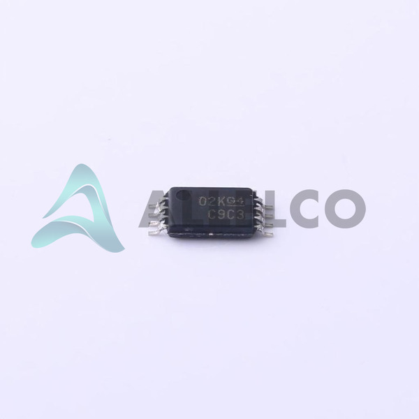
CDCLVC1103PWR (1)
Manufacturer Part Number
CDCLVC1103PWR
Manufacturer
Texas Instruments
Introduction
The CDCLVC1103 is a high-speed fanout buffer designed to distribute high frequency clock signals in electronic systems.
Product Features and Performance
Fanout Buffer (Distribution) type
One input to three output configuration
Supports LVCMOS input and output levels
Operates up to 250 MHz frequency
Wide supply voltage range from 2.3V to 3.6V
Suitable for -40°C to 85°C operating temperature range
Surface Mount 8-TSSOP package ensures compact design
Product Advantages
Low additive phase noise for cleaner clock signal distribution
Capable of operating at high temperatures
Compact package suitable for space-constrained applications
Provides low skew and high signal integrity
CDCLVC1103PWR (2)
Key Technical Parameters
Number of Circuits: 1
Ratio - Input:Output: 1:3
Differential - Input:Output: No/No
Input: LVCMOS
Output: LVCMOS
Frequency - Max: 250 MHz
Voltage - Supply: 2.3V ~ 3.6V
Operating Temperature: -40°C ~ 85°C
Mounting Type: Surface Mount
Package / Case: 8-TSSOP
Supplier Device Package: 8-TSSOP
Quality and Safety Features
Manufactured by a reputable company ensuring reliability and quality
Constructed to operate reliably within specified temperature ranges
Compatibility
Compatible with LVCMOS input and output signal levels
Adaptable for various systems through its wide voltage supply range
Application Areas
Telecommunications
Consumer Electronics
Industrial Control Systems
Networking Equipment
Data Processing
Product Lifecycle
Active product status
Regularly stocked and not nearing discontinuation
Potential future replacements or upgrades available within Texas Instruments' portfolio
Several Key Reasons to Choose This Product
Maintains signal integrity even at high operating frequencies
Eases the design process with a simple 1:3 clock distribution solution
Ensures compatibility with LVCMOS technology
Reduces design footprint due to its small package size
Produced by Texas Instruments, known for quality and support
 CDCLVC1106PWTexas InstrumentsIC CLK BUFFER 1:6 250MHZ 14TSSOP
 CDCLVC1102PWTexas InstrumentsIC CLK BUFFER 1:2 250MHZ 8TSSOP
 CDCLVC1104EVMTexas InstrumentsEVAL MODULE FOR CDCLVC1104
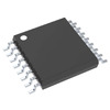 CDCLVC1108PWTexas InstrumentsIC CLK BUFFER 1:8 250MHZ 16TSSOP
 CDCLVC1103PWTexas Instruments
 CDCLD120 TR13Central Semiconductor CorpIC CURRENT LIMITING DPAK
 CDCLVC1103PERTexas Instruments


