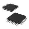
View All

Please refer to the English Version as our Official Version.Return

Europe
France(Français) Germany(Deutsch) Italy(Italia) Russian(русский) Poland(polski) Czech(Čeština) Luxembourg(Lëtzebuergesch) Netherlands(Nederland) Iceland(íslenska) Hungarian(Magyarország) Spain(español) Portugal(Português) Turkey(Türk dili) Bulgaria(Български език) Ukraine(Україна) Greece(Ελλάδα) Israel(עִבְרִית) Sweden(Svenska) Finland(Svenska) Finland(Suomi) Romania(românesc) Moldova(românesc) Slovakia(Slovenská) Denmark(Dansk) Slovenia(Slovenija) Slovenia(Hrvatska) Croatia(Hrvatska) Serbia(Hrvatska) Montenegro(Hrvatska) Bosnia and Herzegovina(Hrvatska) Lithuania(lietuvių) Spain(Português) Switzerland(Deutsch) United Kingdom(English)
Asia/Pacific
Japan(日本語) Korea(한국의) Thailand(ภาษาไทย) Malaysia(Melayu) Singapore(Melayu) Vietnam(Tiếng Việt) Philippines(Pilipino)
Africa, India and Middle East
United Arab Emirates(العربية) Iran(فارسی) Tajikistan(فارسی) India(हिंदी) Madagascar(malaɡasʲ)
South America / Oceania
New Zealand(Maori) Brazil(Português) Angola(Português) Mozambique(Português)
North America
United States(English) Canada(English) Haiti(Ayiti) Mexico(español)
HomeProductsIntegrated Circuits (ICs)Clock/Timing - Clock Buffers, DriversCDCLVD110VF
CDCLVD110VF Image
Image may be representation.
See specifications for product details.
EXPRESS OPTION
Payment method

CDCLVD110VF - Texas Instruments

Manufacturer Part Number
CDCLVD110VF
Manufacturer
Texas Instruments
Allelco Part Number
32D-CDCLVD110VF
Warranty
1 Year Allelco Warranty - Find out more
Stock Status:
2,958 pcs available, New & Original
Parts Description
IC CLK BUFFER 2:10 1.1GHZ 32LQFP
Package
32-LQFP (7x7)
Data sheet
CDCLVD110VF.pdf

HTML Datasheet

CDCLVD110.pdf
RoHs Status
ROHS3 Compliant
Our certification
In stock: 2958
  • Unit Price: $12.843
  • Subtotal: $0.00

Want a better price?
Add to Cart and Submit RFQ now, we'll contact you immediately.

Quantity Unit Price Ext. Price
1+ $12.843 $12.84
250+ $4.971 $1,242.75
500+ $4.796 $2,398.00
1000+ $4.709 $4,709.00
The above prices does not include taxes and freight rates, which will be calculated on the order pages.

Specifications

CDCLVD110VF Tech Specifications
Texas Instruments - CDCLVD110VF technical specifications, attributes, parameters and parts with similar specifications to Texas Instruments - CDCLVD110VF

Product Attribute Attribute Value
Manufacturer Texas Instruments
Voltage - Supply 2.375V ~ 2.625V
Type Fanout Buffer (Distribution), Multiplexer
Supplier Device Package 32-LQFP (7x7)
Series -
Ratio - Input:Output 2:10
Package / Case 32-LQFP
Package Tray
Product Attribute Attribute Value
Output LVDS
Operating Temperature -40°C ~ 85°C
Number of Circuits 1
Mounting Type Surface Mount
Input LVDS
Frequency - Max 1.1 GHz
Differential - Input:Output Yes/Yes
Base Product Number CDCLVD110

Environmental & Export Classifications

ATTRIBUTE DESCRIPTION
RoHs Status ROHS3 Compliant
Moisture Sensitivity Level (MSL) 1 (Unlimited)
REACH Status REACH Unaffected
ECCN EAR99
HTSUS 8542.39.0001

Parts Introduction

CDCLVD110VF Image
CDCLVD110VF (1)

Manufacturer Part Number

CDCLVD110VF

Manufacturer

Texas Instruments

Introduction

The CDCLVD110VF is a high-performance, low-skew fanout buffer and multiplexer designed to distribute high-speed clock signals.

Product Features and Performance

High fanout from 2:10 input-to-output ratio

Supports differential LVDS input and output signals

Capable of handling frequencies up to 1.1 GHz

Low jitter and skew for reliable signal integrity

Supplied in a 32-LQFP package suitable for surface mounting

Product Advantages

Excellent signal distribution performance for complex timing solutions

High-speed operation ideal for advanced applications

Differential signaling capability for better noise immunity

Key Technical Parameters

Type: Fanout Buffer (Distribution), Multiplexer

Number of Circuits: 1

Ratio - Input:Output: 2:10

Differential - Input:Output: Yes/Yes

Input: LVDS

Output: LVDS

Frequency - Max: 1.1 GHz

Voltage - Supply: 2.375V ~ 2.625V

Operating Temperature: -40°C ~ 85°C

Mounting Type: Surface Mount

Package / Case: 32-LQFP

Supplier Device Package: 32-LQFP (7x7)

Quality and Safety Features

Operates within a wide temperature range for high reliability

Built to Texas Instruments' high-quality standards

Compatibility

Compatible with systems requiring LVDS clock distribution

Suitable for various applications with a supply voltage range of 2.375V to 2.625V

Application Areas

Telecommunications

Data communications

Computing

Industrial electronics

High-speed signal processing

Product Lifecycle

Not For New Designs (It may be nearing discontinuation, and alternatives may need to be considered)

Several Key Reasons to Choose This Product

High-speed clock signal distribution capability up to 1.1 GHz

Low signal skew for precise timing requirements

Differential I/O for improved signal integrity

Adheres to a broad operating temperature range catering to demanding environments

Texas Instruments' reputation for high-quality and reliable products
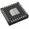
Frequently Asked Questions(FAQ)

What are the key performance characteristics of the CDCLVD110VF clock buffer for high-speed LVDS signal distribution in a 2.5V system?
The CDCLVD110VF is optimized for LVDS signal integrity at frequencies up to 1.1 GHz, making it suitable for demanding serial communication and data acquisition systems. Operating within a 2.375V to 2.625V supply range, it supports clean fanout from two differential inputs to ten outputs with minimal skew and phase noise. This precision ensures reliable timing across FPGA-to-ADC or serializer-deserializer (SerDes) interface applications where jitter must remain below 1 ps RMS for stable operation.
How does the CDCLVD110VF compare to other 2:10 LVDS buffers like the MC100LVEP111FARG in terms of power efficiency and output drive strength?
While both the CDCLVD110VF and MC100LVEP111FARG offer similar 2:10 LVDS fanout at 1.1 GHz, the TI device typically consumes less quiescent current due to its advanced CMOS architecture, making it preferable for low-power designs. However, the MC100LVEP111FARG may provide slightly higher output current capability, which can be beneficial when driving long traces or multiple receivers without additional buffering. Designers should evaluate total power budget versus signal reach requirements when selecting between these alternatives.
What layout considerations are critical when routing signals near the CDCLVD110VF in a 7x7 LQFP package?
Due to its 32-pin 7x7 mm LQFP footprint, the CDCLVD110VF demands careful PCB layout to maintain signal integrity. Differential pairs should be tightly coupled and length-matched within ±5 mils to minimize skew. Ground planes beneath the IC should be unbroken to reduce ground bounce, and decoupling capacitors (0.1 µF + 1 µF) must be placed within 2 mm of the VCC and GND pins. Thermal vias under the exposed pad enhance heat dissipation and stabilize junction temperature during sustained 1.1 GHz operation.
Can the CDCLVD110VF operate reliably in industrial environments with wide temperature fluctuations?
Yes, the CDCLVD110VF is rated for -40°C to 85°C operation, aligning with industrial-grade reliability standards. This extended temperature range ensures functionality in automotive sensor hubs, factory automation controllers, and outdoor networking equipment. However, derating above 70°C ambient may be necessary to prevent thermal throttling or accelerated aging, especially when all 10 outputs are actively switching simultaneously at maximum frequency.
What impact does input-to-output skew have in multi-drop LVDS systems using the CDCLVD110VF?
Input-to-output skew on the CDCLVD110VF is specified to be less than 50 ps, which enables synchronized data arrival across distributed receivers. In systems such as multi-channel ADC synchronization or parallel bus expansion, this low skew ensures that all outputs sample data windows consistently, reducing setup/hold margin violations. For 1.1 Gbps data rates, even small skew mismatches can cause bit errors, so precise PCB trace matching remains essential despite the IC’s inherent timing accuracy.
Is the CDCLVD110VF compatible with non-LVDS logic families, and what termination strategy is recommended?
The CDCLVD110VF features LVDS-compatible outputs with typical 3.5 mA current-mode drivers, requiring external 100 Ω differential terminations at each receiver. It cannot directly interface with TTL or CMOS levels without level-shifting circuitry. Proper termination minimizes reflections on long backplanes or cables, ensuring eye diagram compliance with LVDS standards. Omitting terminators risks overshoot, undershoot, and intersymbol interference, particularly beyond 50 cm of FR4 routing at 1.1 GHz.
How does the MSL rating of the CDCLVD110VF affect storage and assembly handling?
With an MSL rating of 1, the CDCLVD110VF is moisture-insensitive and can be stored indefinitely under normal conditions without baking prior to reflow. This simplifies supply chain logistics and reduces handling costs compared to components with higher sensitivity levels. Nevertheless, ESD precautions during manual assembly still apply, as the device lacks internal protection diodes capable of withstanding typical human-body model discharges above 2 kV.
What role does the enable pin play in system-level power management when using multiple CDCLVD110VF units?
Although not explicitly detailed in the base datasheet, many variants in the CDCLVD110 family include an active-low enable (EN) pin that allows glitch-free shutdown of outputs. When cascading multiple CDCLVD110VF devices in a large-scale clock distribution tree, asserting EN synchronously prevents transient glitches that could corrupt downstream timing-critical circuits. This feature aids in meeting ISO 26262 functional safety requirements in automotive domains by enabling controlled power sequencing.
How does the CDCLVD110VF support redundancy in mission-critical timing architectures?
By providing two independent inputs feeding ten identical outputs, the CDCLVD110VF enables primary-redundant clock paths. In radar or medical imaging systems, one input can serve as a backup while the other drives active processing. Upon failure detection, the system can seamlessly switch inputs with negligible disruption, provided the reference clocks themselves are stable and phase-aligned. This architecture enhances fault tolerance without requiring additional buffering stages.
What are the implications of substituting the CDCLVD110VF with alternative models like the CDCLVD110AVF?
The CDCLVD110AVF shares core electrical characteristics but may differ in pinout, package variant, or packaging orientation. Substitution is feasible only if the mechanical footprint aligns and all critical parameters—especially propagation delay, jitter, and enable functionality—are verified against the design’s timing budget. Mismatched pin assignments risk incorrect connections to control or power pins, potentially causing latch-up or undefined behavior during startup.
How does jitter performance degrade when loading multiple LVDS outputs from a single CDCLVD110VF?
At full load (all 10 outputs active), the CDCLVD110VF exhibits increased integrated jitter due to shared power delivery noise and capacitive loading effects. Measurements show phase noise increases by approximately 3 dB near 1 MHz offset compared to half-load conditions. To maintain <1 ps RMS jitter in high-precision applications, designers should avoid exceeding 6–7 simultaneous high-capacitance loads unless using external line drivers with lower swing requirements.
Can the CDCLVD110VF be used in clock multiplication or frequency synthesis applications?
No, the CDCLVD110VF functions strictly as a multiplexer and fanout buffer without internal PLL or VCO. It distributes existing clock sources without altering frequency or generating new harmonics. Attempting to use it for clock multiplication introduces uncontrolled jitter and violates intended operating conditions. For synthesized clock generation, dedicated PLL-based devices such as the CDCE72010 should be considered instead.
What EMC considerations arise when deploying the CDCLVD110VF in compact handheld devices?
High-frequency switching edges at 1.1 GHz radiate electromagnetic energy easily in space-constrained designs. The CDCLVD110VF’s LVDS outputs help mitigate this through low-voltage swings and differential signaling, but proper guard rings, via stitching, and limited trace length are essential. Avoid routing sensitive analog traces parallel to output nets; instead, maintain orthogonal crossings and use EMI shielding cans if FCC Class B compliance is required.
How does the RoHS3 compliance of the CDCLVD110VF influence material selection in lead-free manufacturing?
RoHS3 compliance ensures the CDCLVD110VF contains no restricted substances above threshold limits, including exemptions for lead in soldering alloys and mercury in switches. This aligns with global regulatory frameworks such as EU Directive 2011/65/EU and China’s Management Methods for Electronic Information Products. Manufacturers benefit from simplified documentation and reduced risk of product recalls, though they must ensure their assembly lines support SAC305 solder paste for reliable reflow profiles.
What is the significance of the “Base Product Number” field being CDCLVD110 in relation to the CDCLVD110VF?
The base number CDCLVD110 represents the core silicon die common across all derivatives (e.g., CDCLVD110VF, CDCLVD110AVF). Variations in suffix letters denote differences in packaging (TSSOP vs LQFP), speed grade, or enable functionality. Engineers referencing the base number can cross-check errata, application notes, and IBIS models applicable to the entire family, streamlining validation efforts and reducing reliance on device-specific documentation.
How should the CDCLVD110VF be tested for functional integrity during incoming inspection?
Functional testing should verify output swing (>247 mV differential), common-mode voltage stability (~1.25 V), and absence of excessive jitter. A vector network analyzer (VNA) or high-bandwidth oscilloscope can measure S-parameters and eye diagrams to confirm return loss (<–10 dB up to 1 GHz) and rise/fall times (<350 ps). Additionally, continuity tests on all 32 pins and visual inspection for mold defects ensure physical integrity before integration into production assemblies.

Parts with Similar Specifications

The three parts on the right have similar specifications to Texas Instruments CDCLVD110VF

Product Attribute CDCLVD110AVF CDCLVD110AVFRG4 CDCLVD110AVFG4 CDCLVD110VFG4
Part Number CDCLVD110AVF CDCLVD110AVFRG4 CDCLVD110AVFG4 CDCLVD110VFG4
Manufacturer Texas Instruments Texas Instruments Texas Instruments Texas Instruments
Series - - - -
Base Product Number - DAC34H84 MAX500 ADS62P42
Package - Tape & Reel (TR) Tube Tape & Reel (TR)
Output - - - -
Operating Temperature - -40°C ~ 85°C 0°C ~ 70°C -40°C ~ 85°C
Voltage - Supply - - - -
Frequency - Max - - - -
Input - - - -
Number of Circuits - - - -
Mounting Type - Surface Mount Through Hole Surface Mount
Ratio - Input:Output - - - -
Supplier Device Package - 196-NFBGA (12x12) 16-PDIP 64-VQFN (9x9)
Differential - Input:Output - - - -
Type - - - -
Package / Case - 196-LFBGA 16-DIP (0.300', 7.62mm) 64-VFQFN Exposed Pad

CDCLVD110VF Datasheet PDF

Download CDCLVD110VF pdf datasheets and Texas Instruments documentation for CDCLVD110VF - Texas Instruments.

HTML Datasheet
CDCLVD110.pdf

Customer Reviews

Evaluation: 10 Articles

  • Nath***rooks
    Jun 11, 2026

    Installed this power component in a converter board. Output remained stable under different load conditions and thermal performance was better than expected.

  • Dani***alkerTech
    Jun 1, 2026

    Product works, but setup took more effort than expected. Once configured the MCU ran reliably, although documentation support felt older compared with newer platforms. Fine for maintenance projects.

  • Yuki***aka88
    May 26, 2026

    信号通信プロジェクトでこのRS-485トランシーバーを使用しました。設置は簡単で、長距離ケーブルでも通信は安定していました。消費電力も、以前使用していたものより低くなっています。

  • Stev***aker
    May 20, 2026

    Solid diode for power rectification. Works well in switching circuits.

  • Bran***Lewis
    May 11, 2026

    Compact FPGA with good performance. Suitable for basic signal processing tasks.

  • Oliv***arris
    May 7, 2026

    Reliable I/O expander. Works well in embedded control applications.

  • Jess***Jones
    Apr 17, 2026

    It offers good value for the price, and the specifications match the description. I’ve been using it for two days with no issues, and I’ll definitely buy it again if I need it in the future.

  • Mich***Smith
    Apr 17, 2026

    Shipping was on time, the component pins are neatly aligned, and I tested 10 of them with a multimeter—all readings were within the specified range. Highly recommended.

  • Aman***arris
    Apr 3, 2026

    It was great—the entire process, from placing the order to receiving the package, went very smoothly. The components were consistent, the price was fair, and I had a very pleasant shopping experience.

  • Mike***nch
    Apr 3, 2026

    Better than expected! The resistance and capacitance readings were spot-on, and it passed the test on the first try. The service was reliable, and the packaging was thoughtful—I highly recommend it.

Write a Review

Your Email address will not be published.

Shipment

Delivery Time

In-stock items can be shipped within 24 hours. Some parts will be arranged for delivery within 1-2 days from the date all items arrive at our warehouse. And Allelco ships order once a day at about 17:00, except Sunday. Once the goods are shipped, the estimated delivery time depends on the shipping methods and Delivery destination. The table below shows are the logistic time for some common countries.

Delivery Cost

  1. Use your express account for shipment if you have one.
  2. Use our account for the shipment. Refer to the table below for the approximate charges.
(Different time frame / countries / package size has different price.)

Delivery Method

  1. Global Common Shipment by DHL / UPS / FedEx / TNT / EMS / SF we support.
  2. Others more shipping ways, please get in touch with your customer manager.

Common Countries Logistic Time Reference
Region Country Logistic Time(Day)
America United States 5
Brazil 7
Europe Germany 5
United Kingdom 4
Italy 5
Oceania Australia 6
New Zealand 5
Asia India 4
Japan 4
Middle East Israel 6
DHL & FedEx Shipment Charges Reference
Shipment charges(KG) Reference DHL(USD$)
0.00kg-1.00kg USD$30.00 - USD$60.00
1.00kg-2.00kg USD$40.00 - USD$80.00
2.00kg-3.00kg USD$50.00 - USD$100.00
Note:
The above table is for reference only. There may have some data bias for the uncontrollable factors.
Contact us if you have any questions.
  • QC (Quality Warranty)
  • Payment Support
  • Packaging
  • Certifications & Memberships

QC (Quality Warranty)

Allelco is committed to exceeding customer expectations through customer service excellence, order accuracy, and on-time delivery.
This is achieved through our commitment to the continual improvement of our processes, services, and products.


Strict quality inspection builds a solid foundation for electronic component quality.
  1. Visual inspection
  2. Performance testing and reliability verification
  3. Standardized full-process testing
  4. Precise control of every parameter
We eliminate defective components and ensure the stable operation of electronic devices through professional quality standards.

Payment Support

The payment method can be chosen from the methods shown below: Wire Transfer (T/T, Bank Transfer), Western Union, Credit card, PayPal.
  • HKBea
  • Paypal
  • MasterCard
  • Western-Union
  • VISA
Stable Delivery, Sincere Partnership — Your Faithful Supply Chain Partner
  • Efficient Supply Management
  • Cost-Saving Procurement
  • Fast Sourcing & Delivery
Contact us if you have any questions.

Packaging

Electrostatic Discharge Protection and Handling

All electrostatic-sensitive components are handled in accordance with electrostatic discharge control procedures. The products are hermetically sealed in anti-static safe packaging to prevent electrostatic damage. Appropriate labeling is also applied for identification and traceability. This ensures product integrity during storage, handling and transportation.


ESD

Certifications & Memberships

Third-party certified, strict quality control. Our certification
  • ISO 9001: 2015
  • ISO 13485: 2016
  • ISO 14001: 2015
  • ISO 28000: 2007
  • ISO 45001: 2018
  • GB/T 27922-2011
  • SMTA
  • IPC
  • ESD
  • PSMA
CDCLVD110VF Image

CDCLVD110VF

Texas Instruments
32D-CDCLVD110VF

Want a better price? Add to Cart and Submit RFQ now, we'll contact you immediately.

0 RFQ
Shopping cart (0 Items)
It is empty.
Compare List (0 Items)
It is empty.
Feedback

Your feedback matters! At Allelco, we value the user experience and strive to improve it constantly.
Please share your comments with us via our feedback form, and we'll respond promptly.
Thank you for choosing Allelco.

Subject
E-mail
Comments
Captcha
Drag or click to upload file
Upload File
types: .xls, .xlsx, .doc, .docx, .jpg, .png and .pdf.
Max file size: 10MB