View All

Please refer to the English Version as our Official Version.Return

Europe
France(Français) Germany(Deutsch) Italy(Italia) Russian(русский) Poland(polski) Czech(Čeština) Luxembourg(Lëtzebuergesch) Netherlands(Nederland) Iceland(íslenska) Hungarian(Magyarország) Spain(español) Portugal(Português) Turkey(Türk dili) Bulgaria(Български език) Ukraine(Україна) Greece(Ελλάδα) Israel(עִבְרִית) Sweden(Svenska) Finland(Svenska) Finland(Suomi) Romania(românesc) Moldova(românesc) Slovakia(Slovenská) Denmark(Dansk) Slovenia(Slovenija) Slovenia(Hrvatska) Croatia(Hrvatska) Serbia(Hrvatska) Montenegro(Hrvatska) Bosnia and Herzegovina(Hrvatska) Lithuania(lietuvių) Spain(Português) Switzerland(Deutsch) United Kingdom(English)
Asia/Pacific
Japan(日本語) Korea(한국의) Thailand(ภาษาไทย) Malaysia(Melayu) Singapore(Melayu) Vietnam(Tiếng Việt) Philippines(Pilipino)
Africa, India and Middle East
United Arab Emirates(العربية) Iran(فارسی) Tajikistan(فارسی) India(हिंदी) Madagascar(malaɡasʲ)
South America / Oceania
New Zealand(Maori) Brazil(Português) Angola(Português) Mozambique(Português)
North America
United States(English) Canada(English) Haiti(Ayiti) Mexico(español)
HomeProductsIntegrated Circuits (ICs)Clock/Timing - Clock Buffers, DriversCDCLVP110VF
CDCLVP110VF Image
Image may be representation.
See specifications for product details.
EXPRESS OPTION
Payment method

CDCLVP110VF - Texas Instruments

Manufacturer Part Number
CDCLVP110VF
Manufacturer
Texas Instruments
Allelco Part Number
32D-CDCLVP110VF
Warranty
1 Year Allelco Warranty - Find out more
Stock Status:
4,286 pcs available, New & Original
Parts Description
IC CLK BUFFER 2:10 3.5GHZ 32LQFP
Package
32-LQFP (7x7)
Data sheet
CDCLVP110VF.pdf
RoHs Status
ROHS3 Compliant
Our certification
In stock: 4286
  • Unit Price: $15.278
  • Subtotal: $0.00

Want a better price?
Add to Cart and Submit RFQ now, we'll contact you immediately.

Quantity Unit Price Ext. Price
1+ $15.278 $15.28
250+ $5.913 $1,478.25
500+ $5.705 $2,852.50
1000+ $5.602 $5,602.00
The above prices does not include taxes and freight rates, which will be calculated on the order pages.

Specifications

CDCLVP110VF Tech Specifications
Texas Instruments - CDCLVP110VF technical specifications, attributes, parameters and parts with similar specifications to Texas Instruments - CDCLVP110VF

Product Attribute Attribute Value
Manufacturer Texas Instruments
Voltage - Supply 2.375V ~ 3.8V
Type Fanout Buffer (Distribution), Multiplexer
Supplier Device Package 32-LQFP (7x7)
Series -
Ratio - Input:Output 2:10
Package / Case 32-LQFP
Package Tray
Product Attribute Attribute Value
Output LVPECL
Operating Temperature -40°C ~ 85°C
Number of Circuits 1
Mounting Type Surface Mount
Input HSTL, LVPECL
Frequency - Max 3.5 GHz
Differential - Input:Output Yes/Yes
Base Product Number CDCLVP110

Environmental & Export Classifications

ATTRIBUTE DESCRIPTION
RoHs Status ROHS3 Compliant
Moisture Sensitivity Level (MSL) 1 (Unlimited)
REACH Status REACH Unaffected
ECCN EAR99
HTSUS 8542.39.0001

Parts Introduction

CDCLVP110VF Image
CDCLVP110VF (1)

Manufacturer Part Number

CDCLVP110VF

Manufacturer

Texas Instruments

Introduction

The CDCLVP110VF is a high-speed, low-power, dual fanout buffer capable of distributing high-speed clocks or differential signals while maintaining signal integrity.

Product Features and Performance

Supports clock frequencies up to 3.5 GHz

Differential input and output interfaces (LVPECL)

2 inputs to 10 outputs fanout

Low power consumption

Superior jitter performance

Tight output-to-output skew

Product Advantages

Enables high-speed clock distribution in high-speed digital systems

Preserves signal integrity of high-speed signals

Compact 32-LQFP package

Key Technical Parameters

Operating voltage: 2.375V to 3.8V

Operating temperature: -40°C to 85°C

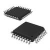
32-LQFP (7x7) package

Quality and Safety Features

RoHS3 compliant

Robust package design for reliable operation

Compatibility

Compatible with HSTL and LVPECL input and output standards

Application Areas

High-speed digital systems

Networking equipment

Telecommunications infrastructure

Server and storage systems

Product Lifecycle

Currently in production

No plans for discontinuation

Replacement or upgrade options available from Texas Instruments

Several Key Reasons to Choose This Product

Supports high-speed clock distribution up to 3.5 GHz

Maintains signal integrity with differential input and output interfaces

Efficient 2:10 fanout ratio

Low power consumption

Compact and reliable 32-LQFP package

RoHS3 compliance for environmental sustainability

Frequently Asked Questions(FAQ)

How does the CDCLVP110VF handle jitter performance at 3.5 GHz when used as a clock distribution buffer in high-speed systems?
The CDCLVP110VF maintains low additive jitter characteristics suitable for sensitive timing applications, with typical output jitter contribution under 1 ps RMS when operating near maximum frequency. This level of jitter is consistent with high-performance LVPECL fanout buffers and supports stable operation in systems requiring phase-coherent clocking across multiple endpoints.
What are the key differences between using the CDCLVP110VF in single-ended versus differential input configurations?
When configured for single-ended HSTL inputs, the CDCLVP110VF provides standard logic-level compatibility but with reduced noise immunity compared to its native differential LVPECL/HSTL support. Differential inputs enable better rejection of common-mode noise and improved signal integrity at frequencies approaching 3.5 GHz, making them preferable in noisy environments or long trace routing scenarios.
Can the CDCLVP110VF drive 10 identical LVPECL loads simultaneously without significant degradation in rise time or amplitude?
Yes, the device is designed to drive up to 10 LVPECL outputs with minimal skew and acceptable signal integrity. However, each load should be treated as a capacitive burden; total capacitive load beyond 20 pF may require careful PCB layout to maintain edge rates above 100 ps. In practice, most designs observe signal degradation only when driving mixed loads or exceeding thermal limits due to increased power dissipation.
How does supply voltage selection affect propagation delay and power consumption in the CDCLVP110VF?
Propagation delay decreases slightly with higher supply voltages within the 2.375V–3.8V range, but the variation is typically less than 10% over this interval. Lower supply voltages reduce dynamic power proportionally, which can improve thermal performance in battery-powered or compact designs. At 3.5 GHz operation, however, margin should be maintained to avoid setup/hold violations due to process variation.
Is the CDCLVP110VF suitable for point-to-multipoint clock distribution in PCIe Gen5 or similar high-bandwidth protocols?
While not protocol-specific, the CDCLVP110VF’s 3.5 GHz bandwidth and low skew make it compatible with PCIe Gen5 timing requirements. Its 2:10 ratio allows efficient tree-based clocking from a single reference. Designers must still ensure total jitter budget compliance, including contributions from upstream sources and PCB channel loss, which may necessitate equalization or reclocking for longer traces.
What precautions should be taken during PCB layout when implementing the CDCLVP110VF in a 7x7 LQFP package?
Minimize stub lengths on all output paths, use controlled impedance traces (typically 50 Ω differential), and place bypass capacitors (0.1 µF) as close as possible to VCC and GND pins. Ground plane continuity beneath the IC is critical for minimizing inductance and EMI. Thermal vias under the exposed pad help dissipate heat during continuous high-frequency operation.
How does temperature variation from -40°C to +85°C impact clock stability in the CDCLVP110VF?
Within the specified operating range, the device maintains stable output frequency with typical drift less than ±50 ppm. Internal biasing and reference circuits compensate adequately across temperature, though extreme corners may see slight increases in propagation delay variance. Long-term reliability remains unaffected due to robust design and absence of volatile tuning elements.
Can the CDCLVP110VF function as both a multiplexer and fanout buffer simultaneously, and what are the implications for unused inputs?
Yes, the part combines multiplexing capability with buffered fanout. Unused inputs should be terminated properly—either differentially or through pull-down resistors—to prevent oscillation or undefined switching. Similarly, unused outputs must be AC-coupled or loaded to maintain signal integrity on active channels. Improper termination can lead to reflections or excessive power draw.
How does the CDCLVP110VF compare to alternative TI devices like the CDCE925 or CDCVF2505 in terms of output count and architecture?
Unlike the CDCE925, which integrates PLLs and VCXO functionality, the CDCLVP110VF is a pure fanout buffer with no frequency synthesis. Compared to the CDCVF2505 (a lower-speed 2.5 GHz buffer), the CDCLVP110VF offers higher bandwidth and greater output count but lacks integrated features such as spread spectrum or programmable delays, making it ideal for fixed-ratio clock trees rather than flexible timing generation.
What role does the Moisture Sensitivity Level (MSL) rating of 1 play in handling and storage of the CDCLVP110VF?
With an MSL of 1, the CDCLVP110VF is considered non-critical regarding moisture exposure and can be stored indefinitely under normal conditions without baking prior to reflow soldering. This simplifies inventory management and reduces assembly risk, especially beneficial for high-volume production environments where lead time and storage logistics are optimized.
Are there any known limitations regarding simultaneous switching noise (SSN) when multiple outputs toggle concurrently on the CDCLVP110VF?
Concurrent switching of multiple LVPECL outputs can generate transient currents that induce ground bounce or supply droop. Proper decoupling, short return paths, and localized power planes mitigate these effects. Designers should simulate peak current demands and verify PDN impedance below 50 mΩ at harmonics of the 3.5 GHz fundamental to avoid timing margins being compromised.
Does the CDCLVP110VF support hot-plugging or dynamic reconfiguration of input source selection?
No, the CDCLVP110VF does not include hot-swap protection or dynamic input switching logic. Input selection must occur while the system is powered and stable. Abrupt changes in input source may cause glitches or brief invalid states, so designers should implement control sequencing in firmware or analog switching circuitry if source redundancy is required.
How does the choice between tray and tape-and-reel packaging affect procurement and assembly for the CDCLVP110VF?
Tray packaging suits low-volume prototyping and repair scenarios, offering easy visual inspection but less automation-friendly handling. Tape-and-reel enables automated pick-and-place assembly and improves handling efficiency in high-volume manufacturing. Both formats maintain identical electrical performance and RoHS compliance, so selection depends solely on production volume and supply chain strategy.
What considerations apply when cascading the CDCLVP110VF in multi-stage clock distribution networks?
Cascading increases total jitter accumulation and cumulative propagation delay. Each stage introduces additive phase noise, so maximum chain length should be limited based on end-to-end jitter budgets. Additionally, loading effects multiply across stages, potentially degrading signal integrity unless buffered effectively. For best results, limit cascading to two or three levels and validate with actual test hardware before committing to production.
How does the ECCN classification of EAR99 influence global sourcing decisions involving the CDCLVP110VF?
Classified as EAR99, the CDCLVP110VF is subject to U.S. export regulations but generally available worldwide without complex licensing, provided it is not integrated into restricted end products. This simplifies international procurement and reduces regulatory overhead, making it attractive for distributed engineering teams and global supply chains.
Can the CDCLVP110VF operate reliably when driven by a non-standard LVPECL signal with asymmetric swing?
The device expects nominal LVPECL swing (approximately 700 mV differential). Asymmetric or attenuated input signals may result in degraded noise margin and potential failure to meet setup/hold timing windows at high frequencies. If non-standard signaling is unavoidable, pre-conditioning via amplification or level-shifting may be required to restore full-compliance waveforms.
What steps should be taken to validate the CDCLVP110VF in a real-world application before mass deployment?
Conduct eye diagram testing at worst-case process-voltage-temperature (PVT) corners, measure total jitter against system specifications, and verify skew consistency across all outputs. Use high-bandwidth oscilloscopes with proper probing techniques to avoid measurement artifacts. Functional validation should include stress tests such as rapid input switching and thermal cycling to uncover subtle timing anomalies not evident in datasheet parameters.
How does the absence of programmable features in the CDCLVP110VF impact flexibility compared to more advanced timing ICs?
The CDCLVP110VF offers fixed 2:10 fanout and deterministic latency, simplifying design and reducing calibration overhead. While this sacrifices configurability (e.g., no delay adjustment or output enable sequencing), it ensures predictable behavior and lower bill-of-materials cost. This trade-off favors systems where timing relationships are fixed and performance predictability outweighs need for runtime adaptability.

Parts with Similar Specifications

The three parts on the right have similar specifications to Texas Instruments CDCLVP110VF

Product Attribute CDCLVP110VFR CDCLVP110MVFRG4 CDCLVP110VFRG4 CDCLVP110VFG4
Part Number CDCLVP110VFR CDCLVP110MVFRG4 CDCLVP110VFRG4 CDCLVP110VFG4
Manufacturer Texas Instruments Texas Instruments Texas Instruments Texas Instruments
Output - - - -
Number of Circuits - - - -
Operating Temperature - -40°C ~ 85°C 0°C ~ 70°C -40°C ~ 85°C
Series - - - -
Supplier Device Package - 196-NFBGA (12x12) 16-PDIP 64-VQFN (9x9)
Ratio - Input:Output - - - -
Base Product Number - DAC34H84 MAX500 ADS62P42
Type - - - -
Differential - Input:Output - - - -
Package / Case - 196-LFBGA 16-DIP (0.300', 7.62mm) 64-VFQFN Exposed Pad
Mounting Type - Surface Mount Through Hole Surface Mount
Input - - - -
Frequency - Max - - - -
Voltage - Supply - - - -
Package - Tape & Reel (TR) Tube Tape & Reel (TR)

CDCLVP110VF Datasheet PDF

Download CDCLVP110VF pdf datasheets and Texas Instruments documentation for CDCLVP110VF - Texas Instruments.

HTML Datasheet
Cylindrical Battery Holders.pdf

Customer Reviews

Evaluation: 10 Articles

  • Nath***rooks
    Jun 11, 2026

    Installed this power component in a converter board. Output remained stable under different load conditions and thermal performance was better than expected.

  • Dani***alkerTech
    Jun 1, 2026

    Product works, but setup took more effort than expected. Once configured the MCU ran reliably, although documentation support felt older compared with newer platforms. Fine for maintenance projects.

  • Yuki***aka88
    May 26, 2026

    信号通信プロジェクトでこのRS-485トランシーバーを使用しました。設置は簡単で、長距離ケーブルでも通信は安定していました。消費電力も、以前使用していたものより低くなっています。

  • Stev***aker
    May 20, 2026

    Solid diode for power rectification. Works well in switching circuits.

  • Bran***Lewis
    May 11, 2026

    Compact FPGA with good performance. Suitable for basic signal processing tasks.

  • Oliv***arris
    May 7, 2026

    Reliable I/O expander. Works well in embedded control applications.

  • Jess***Jones
    Apr 17, 2026

    It offers good value for the price, and the specifications match the description. I’ve been using it for two days with no issues, and I’ll definitely buy it again if I need it in the future.

  • Mich***Smith
    Apr 17, 2026

    Shipping was on time, the component pins are neatly aligned, and I tested 10 of them with a multimeter—all readings were within the specified range. Highly recommended.

  • Aman***arris
    Apr 3, 2026

    It was great—the entire process, from placing the order to receiving the package, went very smoothly. The components were consistent, the price was fair, and I had a very pleasant shopping experience.

  • Mike***nch
    Apr 3, 2026

    Better than expected! The resistance and capacitance readings were spot-on, and it passed the test on the first try. The service was reliable, and the packaging was thoughtful—I highly recommend it.

Write a Review

Your Email address will not be published.

Shipment

Delivery Time

In-stock items can be shipped within 24 hours. Some parts will be arranged for delivery within 1-2 days from the date all items arrive at our warehouse. And Allelco ships order once a day at about 17:00, except Sunday. Once the goods are shipped, the estimated delivery time depends on the shipping methods and Delivery destination. The table below shows are the logistic time for some common countries.

Delivery Cost

  1. Use your express account for shipment if you have one.
  2. Use our account for the shipment. Refer to the table below for the approximate charges.
(Different time frame / countries / package size has different price.)

Delivery Method

  1. Global Common Shipment by DHL / UPS / FedEx / TNT / EMS / SF we support.
  2. Others more shipping ways, please get in touch with your customer manager.

Common Countries Logistic Time Reference
Region Country Logistic Time(Day)
America United States 5
Brazil 7
Europe Germany 5
United Kingdom 4
Italy 5
Oceania Australia 6
New Zealand 5
Asia India 4
Japan 4
Middle East Israel 6
DHL & FedEx Shipment Charges Reference
Shipment charges(KG) Reference DHL(USD$)
0.00kg-1.00kg USD$30.00 - USD$60.00
1.00kg-2.00kg USD$40.00 - USD$80.00
2.00kg-3.00kg USD$50.00 - USD$100.00
Note:
The above table is for reference only. There may have some data bias for the uncontrollable factors.
Contact us if you have any questions.
  • QC (Quality Warranty)
  • Payment Support
  • Packaging
  • Certifications & Memberships

QC (Quality Warranty)

Allelco is committed to exceeding customer expectations through customer service excellence, order accuracy, and on-time delivery.
This is achieved through our commitment to the continual improvement of our processes, services, and products.


Strict quality inspection builds a solid foundation for electronic component quality.
  1. Visual inspection
  2. Performance testing and reliability verification
  3. Standardized full-process testing
  4. Precise control of every parameter
We eliminate defective components and ensure the stable operation of electronic devices through professional quality standards.

Payment Support

The payment method can be chosen from the methods shown below: Wire Transfer (T/T, Bank Transfer), Western Union, Credit card, PayPal.
  • HKBea
  • Paypal
  • MasterCard
  • Western-Union
  • VISA
Stable Delivery, Sincere Partnership — Your Faithful Supply Chain Partner
  • Efficient Supply Management
  • Cost-Saving Procurement
  • Fast Sourcing & Delivery
Contact us if you have any questions.

Packaging

Electrostatic Discharge Protection and Handling

All electrostatic-sensitive components are handled in accordance with electrostatic discharge control procedures. The products are hermetically sealed in anti-static safe packaging to prevent electrostatic damage. Appropriate labeling is also applied for identification and traceability. This ensures product integrity during storage, handling and transportation.


ESD

Certifications & Memberships

Third-party certified, strict quality control. Our certification
  • ISO 9001: 2015
  • ISO 13485: 2016
  • ISO 14001: 2015
  • ISO 28000: 2007
  • ISO 45001: 2018
  • GB/T 27922-2011
  • SMTA
  • IPC
  • ESD
  • PSMA
CDCLVP110VF Image

CDCLVP110VF

Texas Instruments
32D-CDCLVP110VF

Want a better price? Add to Cart and Submit RFQ now, we'll contact you immediately.

0 RFQ
Shopping cart (0 Items)
It is empty.
Compare List (0 Items)
It is empty.
Feedback

Your feedback matters! At Allelco, we value the user experience and strive to improve it constantly.
Please share your comments with us via our feedback form, and we'll respond promptly.
Thank you for choosing Allelco.

Subject
E-mail
Comments
Captcha
Drag or click to upload file
Upload File
types: .xls, .xlsx, .doc, .docx, .jpg, .png and .pdf.
Max file size: 10MB