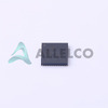
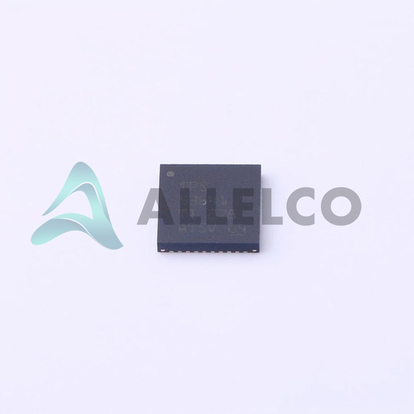
CSD95496QVM (1)
Manufacturer Part Number
CSD95496QVM
Manufacturer
Texas Instruments
Introduction
The CSD95496QVM is a high-performance, full half-bridge driver designed by Texas Instruments, aiming to enhance power management efficiency in a broad range of applications. It is part of the NexFET™ series, signifying innovations in Power MOSFET technology.
Product Features and Performance
Integrated half-bridge (3 output) configuration
Specifically tailored for synchronous buck converters
Employs PWM interface for enhanced control
Supports both inductive and capacitive load types
Utilizes Power MOSFET technology for efficient switching
High current capacity with 40A continuous and 60A peak output
Low supply voltage range of 4.5V to 5.5V, with load voltage handling from 4.5V to 16V
Operating temperature range of -40°C to 125°C, ensuring stability under extreme conditions
Features bootstrap circuit for higher efficiency
Shoot-through fault protection to increase device and system safety
Product Advantages
The integration of bootstrap and fault protection circuits reduces external component needs, simplifying design and lowering system costs.
High current capacity makes it suitable for power-heavy applications.
PWM interface enables precise control over power delivery and efficiency.
Wide operating temperature range ensures reliability across various environments.
Key Technical Parameters
Output configuration: Half Bridge (3)
Interface: PWM
Current Output / Channel: 40A
Current Peak Output: 60A
Voltage Supply: 4.5V ~ 5.5V
Voltage Load: 4.5V ~ 16V
Operating Temperature: -40°C ~ 125°C (TJ)
Quality and Safety Features
Shoot-through fault protection secures the system against potential damages due to erroneous signals or conditions.
Robust Power MOSFET technology ensures durability and high performance under different operational stresses.
Compatibility
With its versatile load and voltage range, the CSD95496QVM is compatible with a wide array of synchronous buck converter designs and applications.
Application Areas
Power supplies
Computing systems
Networking equipment
Industrial machinery
Renewable energy systems
Product Lifecycle
Active status implies ongoing production and availability.
Its presence in Texas Instruments' NexFET™ series suggests continuous support and potential for future upgrades, rather than nearing discontinuation.
Several Key Reasons to Choose This Product
High performance and reliability supported by Texas Instruments' reputation and the NexFET™ series innovations.
Integrated protection features reduce risk and enhance system safety.
Versatile application potential, from industrial machinery to renewable energy systems.
Active product status ensures availability and manufacturer support.
PWM interface and high current capacity allow for precise control and application in high-demand environments.


 CSD95492QVMTTexas InstrumentsIC HALF BRIDGE DRIVER 20A 18VSON
 CSD97374Q4MTexas InstrumentsIC HALF BRIDGE DRIVER 25A 8VSON
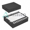 CSD96371Q5MTexas InstrumentsIC HALF BRIDGE DRIVER 50A 22LSON
 CSD97370Q5MTexas InstrumentsIC HALF BRIDGE DRIVER 40A 22LSON


