
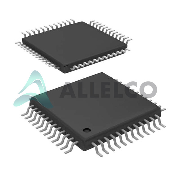
DAC5652AIPFB (1)
Manufacturer Part Number
DAC5652AIPFB
Manufacturer
Texas Instruments
Introduction
DAC5652AIPFB is a dual 10-bit Digital to Analog Converter (DAC) designed for data acquisition applications.
Product Features and Performance
10-bit resolution
Two D/A converters
Settling Time: 20ns (Typical)
Current output type: Unbuffered
Differential output capable
Parallel data interface
Supports both external and internal reference types
Current source architecture
Product Advantages
High-speed performance with a settling time of just 20ns
Precision outputs with differential capabilities enhance signal integrity
Flexible reference type selection including external and internal options
Supports efficient communication via a parallel interface
Key Technical Parameters
Voltage Supply (Analog and Digital): 3V to 3.6V
Number of Bits: 10
Number of D/A Converters: 2
Settling Time: 20ns
INL/DNL (LSB): ±0.25, ±0.03
Operating Temperature: -40°C to 85°C
Quality and Safety Features
Manufactured under high standards ensuring reliable performance
Built to withstand a wide range of operating temperatures
Compatibility
Compatible with various microcontrollers and digital systems using parallel interfaces
Application Areas
Telecommunications
Signal processing
Data acquisition systems
Industrial control systems
Product Lifecycle
Currently active with a stable supply
No near discontinuation indicated
Several Key Reasons to Choose This Product
High-speed operations with minimal settling time enhance efficiency
Dual DACs facilitate multitasking in complex systems
Robust performance in harsh environments with a broad operational temperature range
Flexible reference voltage settings cater to specific application needs
Quality and reliability backed by Texas Instruments' reputation

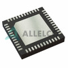 DAC5652AIRSLTTexas InstrumentsIC DAC 10BIT A-OUT 48VQFN
 DAC5578SPWRTexas InstrumentsIC DAC 8BIT V-OUT 16TSSOP
 DAC5578SRGERTexas InstrumentsIC DAC 8BIT V-OUT 24VQFN
 DAC5578SPWTexas InstrumentsIC DAC 8BIT V-OUT 16TSSOP
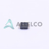 DAC5574IDGSRTexas InstrumentsIC DAC 8BIT V-OUT 10VSSOP
 DAC5652EVMTexas InstrumentsEVALUATION MODULE FOR DAC5652
 DAC5652AEVMTexas InstrumentsDEVELOPMENT DATA ACQUISITION


