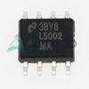
View All

Please refer to the English Version as our Official Version.Return

Europe
France(Français) Germany(Deutsch) Italy(Italia) Russian(русский) Poland(polski) Czech(Čeština) Luxembourg(Lëtzebuergesch) Netherlands(Nederland) Iceland(íslenska) Hungarian(Magyarország) Spain(español) Portugal(Português) Turkey(Türk dili) Bulgaria(Български език) Ukraine(Україна) Greece(Ελλάδα) Israel(עִבְרִית) Sweden(Svenska) Finland(Svenska) Finland(Suomi) Romania(românesc) Moldova(românesc) Slovakia(Slovenská) Denmark(Dansk) Slovenia(Slovenija) Slovenia(Hrvatska) Croatia(Hrvatska) Serbia(Hrvatska) Montenegro(Hrvatska) Bosnia and Herzegovina(Hrvatska) Lithuania(lietuvių) Spain(Português) Switzerland(Deutsch) United Kingdom(English)
Asia/Pacific
Japan(日本語) Korea(한국의) Thailand(ภาษาไทย) Malaysia(Melayu) Singapore(Melayu) Vietnam(Tiếng Việt) Philippines(Pilipino)
Africa, India and Middle East
United Arab Emirates(العربية) Iran(فارسی) Tajikistan(فارسی) India(हिंदी) Madagascar(malaɡasʲ)
South America / Oceania
New Zealand(Maori) Brazil(Português) Angola(Português) Mozambique(Português)
North America
United States(English) Canada(English) Haiti(Ayiti) Mexico(español)
HomeProductsIntegrated Circuits (ICs)PMIC - Voltage Regulators - DC DC Switching RegulatorsLM5002MAX
LM5002MAX Image
Image may be representation.
See specifications for product details.
EXPRESS OPTION
Payment method

LM5002MAX - Texas Instruments

Manufacturer Part Number
LM5002MAX
Manufacturer
Texas Instruments
Allelco Part Number
32D-LM5002MAX
Warranty
1 Year Allelco Warranty - Find out more
Stock Status:
13,718 pcs available, New & Original
Parts Description
IC REG MULTI CONFG ADJ 8SOIC
Package
8-SOIC
Data sheet
LM5002MAX.pdf

HTML Datasheet

LM5002.pdf
RoHs Status
 
Our certification
In stock: 13718

Required fields are indicated by an asterisk (*)
Please send RFQ, we will respond immediately.

Quantity

Specifications

LM5002MAX Tech Specifications
Texas Instruments - LM5002MAX technical specifications, attributes, parameters and parts with similar specifications to Texas Instruments - LM5002MAX

Product Attribute Attribute Value
Manufacturer Texas Instruments
Voltage - Output (Min/Fixed) 3.1V
Voltage - Output (Max) 76V (Switch)
Voltage - Input (Min) 3.1V
Voltage - Input (Max) 75V
Topology Boost, Flyback, Forward Converter, SEPIC
Synchronous Rectifier No
Supplier Device Package 8-SOIC
Series -
Package / Case 8-SOIC (0.154', 3.90mm Width)
Product Attribute Attribute Value
Package Tape & Reel (TR)
Output Type Adjustable
Output Configuration Positive, Isolation Capable
Operating Temperature -40°C ~ 125°C (TJ)
Number of Outputs 1
Mounting Type Surface Mount
Function Step-Up, Step-Up/Step-Down
Frequency - Switching 50kHz ~ 1.5MHz
Current - Output 400mA (Switch)
Base Product Number LM5002

Environmental & Export Classifications

ATTRIBUTE DESCRIPTION
RoHs Status RoHS non-compliant
Moisture Sensitivity Level (MSL) 1 (Unlimited)
REACH Status REACH Unaffected
ECCN EAR99
HTSUS 8542.39.0001

Parts Introduction

LM5002MAX Image
LM5002MAX (1)

Manufacturer Part Number

LM5002MAX

Manufacturer

Texas Instruments

Introduction

High voltage switch mode regulator for power conversion applications

Product Features and Performance

Adjustable output voltage

Highly flexible switching frequency from 50kHz to 1.5MHz

Integrated features for enhanced power management

Product Advantages

Capable of multiple topologies including Boost, Flyback, Forward Converter, SEPIC

Support for a broad range of input and output voltages

Thermal shutdown and current limit protection

LM5002MAX Image
LM5002MAX (2)

Key Technical Parameters

Input Voltage Range: 3.1V to 75V

Output Voltage Range: 3.1V to 76V (Switch)

Output Current: 400mA (Switch)

Switching Frequency: 50kHz to 1.5MHz

Operating Temperature Range: -40°C to 125°C

Quality and Safety Features

Overcurrent protection

Thermal shutdown

Under-voltage lockout

Compatibility

Surface Mount 8-SOIC package compatible with various PCB designs

Application Areas

Telecom infrastructure

Industrial power supplies

Automotive systems

Portable electronics

Product Lifecycle

Not For New Designs

Availability of replacements or upgrades to be determined

Several Key Reasons to Choose This Product

Versatility in handling different power conversion needs

High efficiency potential due to flexible switching options

Robust safety features ensure reliability under various conditions

Wide range of supported input and output voltages for diverse applications

Extended operating temperature range suitable for challenging environments

Frequently Asked Questions(FAQ)

How does the LM5002MAX perform when transitioning between boost and SEPIC modes under variable load conditions, and what design considerations are necessary to maintain stability?
The LM5002MAX supports seamless topology transitions across boost, flyback, forward converter, and SEPIC configurations, but mode switching introduces challenges in feedback loop compensation. When operating near boundary conditions—such as light loads with high input-to-output voltage differentials—the discontinuous conduction mode (DCM) to continuous conduction mode (CCM) transitions can cause audible noise or output ripple spikes. For reliable operation, engineers should implement a Type II compensation network with sufficient phase margin (>45°) and avoid aggressive transient response settings. In SEPIC applications, the shared inductor current path increases cross-regulation sensitivity, requiring careful PCB layout and decoupling to minimize parasitic inductance.
What are the key differences between using the LM5002MAX in a standard boost configuration versus a flyback setup, particularly regarding transformer design and isolation requirements?
In a non-isolated boost application, the LM5002MAX drives an external MOSFET that switches the input voltage directly across the inductor, enabling high efficiency at moderate duty cycles. However, when configured for flyback operation—especially in isolated designs—the device uses the same switch to transfer energy through a transformer during the on-time and store it for release during off-time. This necessitates precise transformer design with tight coupling (k > 0.95), proper turns ratio based on Vin(min)/Vout, and careful management of leakage inductance via snubbers. Unlike boost converters, flyback topologies require secondary-side feedback or optocouplers for regulation, adding complexity and cost. The LM5002MAX supports both, but isolation demands stricter thermal and creepage distance compliance.
Can the LM5002MAX drive multiple outputs simultaneously without degrading performance, and what limitations apply when cascading regulators?
The LM5002MAX is designed for single-output control; it cannot natively manage multiple independent regulated rails from a single IC. Attempting to use it in a multi-rail system without external post-regulators risks poor line and load regulation due to feedback sensing only one node. If multiple outputs are needed, designers must either use discrete post-regulators (e.g., LDOs) or implement a master-slave scheme where the primary output powers auxiliary circuits. Cascading without isolation may also violate EMI standards or introduce ground loops. For applications like industrial power supplies requiring dual rails, this limitation makes the LM5002MAX less suitable than integrated multi-output PMICs.
How does the LM5002MAX handle startup inrush current when connected to high-voltage inputs above 48V, and what protection mechanisms are built-in?
At startup, especially from high input voltages (e.g., 60V), the LM5002MAX’s internal soft-start circuitry limits the ramp rate of the control voltage to prevent excessive gate drive slew, which reduces peak switching current and minimizes stress on external components. However, the input capacitor charging current remains unregulated until the IC begins switching. Therefore, bulk input capacitance should be carefully selected—typically ≤10µF ceramic or low-ESR electrolytic—to avoid tripping overcurrent protection or damaging the IC. No dedicated inrush limiter exists internally, so external NTC thermistors or active PTC-based solutions are recommended for systems exceeding 40V in-rush scenarios.
What impact does switching frequency selection have on efficiency and component size when designing with the LM5002MAX, and how should frequency be chosen for a 75V input to 12V/1A output?
Higher switching frequencies (e.g., >1MHz) allow smaller inductors and capacitors but increase switching losses due to higher MOSFET gate charge dissipation and core losses in magnetic components. For a 75V-to-12V conversion at 1A, choosing 500kHz balances these trade-offs: it enables use of compact shielded inductors (≈47µH) while keeping conduction losses manageable. At 1.5MHz, efficiency drops by ~3–5% due to increased switching losses, though board area shrinks significantly. The LM5002MAX’s adjustable oscillator allows fine-tuning, but optimal frequency depends on MOSFET RDS(on), diode recovery characteristics, and thermal constraints. Always simulate with Spice models accounting for real-world parasitics.
Is it feasible to operate the LM5002MAX near its maximum input voltage of 75V continuously, and what derating practices are advised for reliability?
Continuous operation at 75V is permitted within the absolute maximum rating, but long-term reliability degrades due to elevated junction temperatures and stress on internal pass elements. TI recommends staying below 60V continuous for extended use, applying a 20–30% derating margin. This ensures adequate margin against transients, manufacturing tolerances, and aging effects. Additionally, ensure proper heatsinking if ambient temperatures exceed 70°C, as thermal resistance from junction to ambient (θJA) in SOIC package exceeds 100°C/W. Derating improves mean time between failures (MTBF) and prevents premature latch-up or oxide breakdown.
How does the absence of synchronous rectification in the LM5002MAX affect efficiency in high-current flyback applications compared to alternatives?
Without synchronous rectification, the secondary side relies on a fast-recovery or Schottky diode, introducing forward voltage drop losses (typically 0.4–1.2V depending on current and part). In a 1A flyback converter converting 48V to 12V, this results in ~5–10% lower efficiency than a comparable Synchronous Rectified (SR) design, where a low-RDS(on) MOSFET replaces the diode, reducing conduction loss to <0.1V equivalent. While the LM5002MAX lacks SR support, workarounds exist using external controllers like the LM5108 for the secondary stage, but this adds cost and complexity. For moderate currents (<500mA), the diode solution remains acceptable, but above that threshold, efficiency penalties become significant.
What layout precautions are critical when routing high-voltage traces adjacent to the LM5002MAX in a mixed-signal PCB?
Due to the wide input voltage range (3.1V–75V), creepage and clearance distances between primary high-voltage nodes and sensitive analog signals must meet safety standards (e.g., IEC 60950/62368). Maintain at least 8mm air gap and 4mm copper separation between HV traces and feedback paths, VCC bypass networks, or compensation pins. Use a solid ground plane beneath the IC to shield switching noise, and route SW node traces short and wide to minimize loop area. Place input/output capacitors as close as possible to respective pads. Failure to adhere increases radiated emissions and risks arcing or capacitive coupling into control logic, potentially causing false triggering or instability.
Why might the LM5002MAX exhibit instability when used in a SEPIC configuration with tightly coupled inductors, and how can this be mitigated?
SEPIC converters inherently have two energy storage elements (inductor and coupled capacitor), creating a double-pole system that complicates feedback stabilization. Tight coupling (k ≈ 1) exacerbates this by increasing interaction between windings, leading to peaking in the gain curve and reduced phase margin. With the LM5002MAX, inadequate phase lead in the compensation network often results in oscillations during load steps. Mitigation strategies include using moderate coupling (k ≥ 0.9), adding series resistance to the coupled capacitor to dampen resonance, or redesigning compensation with a zero placed appropriately in the left-half plane. Simulation tools like WEBENCH or LTspice are essential for verifying stability before layout.
How does the LM5002MAX compare to the LM5001 in terms of topology flexibility and suitability for isolated vs. non-isolated designs?
The LM5001 is functionally similar but limited to buck-boost and SEPIC topologies, lacking native support for flyback and forward converters. In contrast, the LM5002MAX extends flexibility by integrating drivers capable of handling transformer-based isolated topologies directly. This makes the LM5002MAX more suitable for industrial isolated supplies, telecom backplanes, or battery-powered systems requiring wide input ranges. However, the LM5001 achieves marginally better efficiency in non-isolated SEPIC apps due to simpler gate drive requirements. Both share identical pinouts and control interfaces, so migration is straightforward—but only the LM5002MAX supports true flyback operation without external controller assistance.
What role does the internal reference voltage play in determining output accuracy across temperature, and how stable is the LM5002MAX’s feedback loop?
The LM5002MAX uses a 1.23V bandgap reference with ±1% initial tolerance, drifting approximately ±50ppm/°C over the -40°C to 125°C range. Combined with resistor divider tolerance (±1%), worst-case output error reaches ±3%. For precision applications (e.g., 12V rail requiring ±2%), external reference buffers or precision resistors are advisable. The internal error amplifier has high open-loop gain (>80dB), ensuring closed-loop stability under most conditions, but phase margin degrades near unity-gain bandwidth if compensation is poorly tuned. Temperature-induced drift is negligible compared to resistive effects, so focus should remain on divider quality rather than relying solely on IC stability.
Can the LM5002MAX be safely used in automotive environments meeting AEC-Q100 standards, and what modifications are needed?
The LM5002MAX is not qualified to AEC-Q100 Grade 1 (-40°C to +125°C) despite operating over that range; it lacks automotive-grade packaging, extended temperature testing, and failure mechanism screening. Using it in automotive systems voids warranty and risks field failures. For certified designs, select TI’s automotive-qualified counterpart (if available) or implement rigorous derating, conformal coating, and environmental testing. Additionally, ensure input surge compliance per ISO 7637-2, which may necessitate TVS diodes rated for 80V+ transients. Non-automotive use remains acceptable, but claiming functional safety certification without qualification is inappropriate.

Parts with Similar Specifications

The three parts on the right have similar specifications to Texas Instruments LM5002MAX

Product Attribute LM5002MA LM5002SDX LM5002SD LM5001SDX
Part Number LM5002MA LM5002SDX LM5002SD LM5001SDX
Manufacturer Texas Instruments Texas Instruments Texas Instruments Texas Instruments
Voltage - Input (Max) - - - -
Mounting Type - Surface Mount Through Hole Surface Mount
Output Type - Current - Unbuffered Voltage - Buffered -
Number of Outputs - - - -
Topology - - - -
Function - - - -
Frequency - Switching - - - -
Supplier Device Package - 196-NFBGA (12x12) 16-PDIP 64-VQFN (9x9)
Voltage - Output (Max) - - - -
Operating Temperature - -40°C ~ 85°C 0°C ~ 70°C -40°C ~ 85°C
Current - Output - - - -
Series - - - -
Synchronous Rectifier - - - -
Package - Tape & Reel (TR) Tube Tape & Reel (TR)
Package / Case - 196-LFBGA 16-DIP (0.300', 7.62mm) 64-VFQFN Exposed Pad
Voltage - Output (Min/Fixed) - - - -
Output Configuration - - - -
Base Product Number - DAC34H84 MAX500 ADS62P42
Voltage - Input (Min) - - - -

LM5002MAX Datasheet PDF

Download LM5002MAX pdf datasheets and Texas Instruments documentation for LM5002MAX - Texas Instruments.

HTML Datasheet
LM5002.pdf

Customer Reviews

Evaluation: 10 Articles

  • Nath***rooks
    Jun 11, 2026

    Installed this power component in a converter board. Output remained stable under different load conditions and thermal performance was better than expected.

  • Dani***alkerTech
    Jun 1, 2026

    Product works, but setup took more effort than expected. Once configured the MCU ran reliably, although documentation support felt older compared with newer platforms. Fine for maintenance projects.

  • Yuki***aka88
    May 26, 2026

    信号通信プロジェクトでこのRS-485トランシーバーを使用しました。設置は簡単で、長距離ケーブルでも通信は安定していました。消費電力も、以前使用していたものより低くなっています。

  • Stev***aker
    May 20, 2026

    Solid diode for power rectification. Works well in switching circuits.

  • Bran***Lewis
    May 11, 2026

    Compact FPGA with good performance. Suitable for basic signal processing tasks.

  • Oliv***arris
    May 7, 2026

    Reliable I/O expander. Works well in embedded control applications.

  • Jess***Jones
    Apr 17, 2026

    It offers good value for the price, and the specifications match the description. I’ve been using it for two days with no issues, and I’ll definitely buy it again if I need it in the future.

  • Mich***Smith
    Apr 17, 2026

    Shipping was on time, the component pins are neatly aligned, and I tested 10 of them with a multimeter—all readings were within the specified range. Highly recommended.

  • Aman***arris
    Apr 3, 2026

    It was great—the entire process, from placing the order to receiving the package, went very smoothly. The components were consistent, the price was fair, and I had a very pleasant shopping experience.

  • Mike***nch
    Apr 3, 2026

    Better than expected! The resistance and capacitance readings were spot-on, and it passed the test on the first try. The service was reliable, and the packaging was thoughtful—I highly recommend it.

Write a Review

Your Email address will not be published.

Shipment

Delivery Time

In-stock items can be shipped within 24 hours. Some parts will be arranged for delivery within 1-2 days from the date all items arrive at our warehouse. And Allelco ships order once a day at about 17:00, except Sunday. Once the goods are shipped, the estimated delivery time depends on the shipping methods and Delivery destination. The table below shows are the logistic time for some common countries.

Delivery Cost

  1. Use your express account for shipment if you have one.
  2. Use our account for the shipment. Refer to the table below for the approximate charges.
(Different time frame / countries / package size has different price.)

Delivery Method

  1. Global Common Shipment by DHL / UPS / FedEx / TNT / EMS / SF we support.
  2. Others more shipping ways, please get in touch with your customer manager.

Common Countries Logistic Time Reference
Region Country Logistic Time(Day)
America United States 5
Brazil 7
Europe Germany 5
United Kingdom 4
Italy 5
Oceania Australia 6
New Zealand 5
Asia India 4
Japan 4
Middle East Israel 6
DHL & FedEx Shipment Charges Reference
Shipment charges(KG) Reference DHL(USD$)
0.00kg-1.00kg USD$30.00 - USD$60.00
1.00kg-2.00kg USD$40.00 - USD$80.00
2.00kg-3.00kg USD$50.00 - USD$100.00
Note:
The above table is for reference only. There may have some data bias for the uncontrollable factors.
Contact us if you have any questions.
  • QC (Quality Warranty)
  • Payment Support
  • Packaging
  • Certifications & Memberships

QC (Quality Warranty)

Allelco is committed to exceeding customer expectations through customer service excellence, order accuracy, and on-time delivery.
This is achieved through our commitment to the continual improvement of our processes, services, and products.


Strict quality inspection builds a solid foundation for electronic component quality.
  1. Visual inspection
  2. Performance testing and reliability verification
  3. Standardized full-process testing
  4. Precise control of every parameter
We eliminate defective components and ensure the stable operation of electronic devices through professional quality standards.

Payment Support

The payment method can be chosen from the methods shown below: Wire Transfer (T/T, Bank Transfer), Western Union, Credit card, PayPal.
  • HKBea
  • Paypal
  • MasterCard
  • Western-Union
  • VISA
Stable Delivery, Sincere Partnership — Your Faithful Supply Chain Partner
  • Efficient Supply Management
  • Cost-Saving Procurement
  • Fast Sourcing & Delivery
Contact us if you have any questions.

Packaging

Electrostatic Discharge Protection and Handling

All electrostatic-sensitive components are handled in accordance with electrostatic discharge control procedures. The products are hermetically sealed in anti-static safe packaging to prevent electrostatic damage. Appropriate labeling is also applied for identification and traceability. This ensures product integrity during storage, handling and transportation.


ESD

Certifications & Memberships

Third-party certified, strict quality control. Our certification
  • ISO 9001: 2015
  • ISO 13485: 2016
  • ISO 14001: 2015
  • ISO 28000: 2007
  • ISO 45001: 2018
  • GB/T 27922-2011
  • SMTA
  • IPC
  • ESD
  • PSMA
LM5002MAX Image

LM5002MAX

Texas Instruments
32D-LM5002MAX

Want a better price? Add to Cart and Submit RFQ now, we'll contact you immediately.

0 RFQ
Shopping cart (0 Items)
It is empty.
Compare List (0 Items)
It is empty.
Feedback

Your feedback matters! At Allelco, we value the user experience and strive to improve it constantly.
Please share your comments with us via our feedback form, and we'll respond promptly.
Thank you for choosing Allelco.

Subject
E-mail
Comments
Captcha
Drag or click to upload file
Upload File
types: .xls, .xlsx, .doc, .docx, .jpg, .png and .pdf.
Max file size: 10MB