LM5009ASD (1)
Manufacturer Part Number
LM5009ASD
Manufacturer
Texas Instruments
Introduction
The LM5009ASD is a high-voltage, step-down DC/DC switching regulator integrated circuit (IC) from Texas Instruments.
Product Features and Performance
Wide input voltage range of 6V to 95V
Adjustable output voltage from 2.5V to 95V
Up to 150mA output current capability
Switching frequency range of 50kHz to 1.1MHz
High-side and low-side MOSFET drivers for synchronous operation
Undervoltage lockout, cycle-by-cycle current limit, and thermal shutdown protection
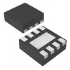
Small 8-pin WDFN (4mm x 4mm) package
Product Advantages
Wide input voltage range allows use in a variety of applications
Adjustable output voltage provides flexibility
High-efficiency synchronous operation improves power conversion
Comprehensive protection features ensure reliable operation
Key Technical Parameters
Input Voltage Range: 6V to 95V
Output Voltage Range: 2.5V to 95V
Output Current: Up to 150mA
Switching Frequency: 50kHz to 1.1MHz
Package: 8-pin WDFN (4mm x 4mm)
Quality and Safety Features
Undervoltage lockout, cycle-by-cycle current limit, and thermal shutdown protection
RoHS non-compliant
Compatibility
The LM5009ASD is compatible with a wide range of electronic devices and systems that require a high-voltage, step-down DC/DC power supply.
Application Areas
Industrial equipment
Automotive electronics
Telecommunications equipment
Medical devices
Instrumentation and control systems
Product Lifecycle
The LM5009ASD is an active product from Texas Instruments. Replacement or upgraded products may be available in the future as technology advances.
Key Reasons to Choose the LM5009ASD
Wide input voltage range of 6V to 95V
Adjustable output voltage from 2.5V to 95V
High-efficiency synchronous operation
Comprehensive protection features for reliable operation
Small 8-pin WDFN (4mm x 4mm) package

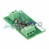 LM5009EVALTexas InstrumentsBOARD EVALUATION LM5009
 LM5009AMMXTexas Instruments
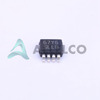 LM5009MMTexas InstrumentsIC REG BUCK ADJ 150MA 8VSSOP
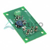 LM5009AEVAL/NOPBTexas InstrumentsEVAL BOARD FOR LM5009A
 LM5008SDCX/NOPBTexas Instruments


