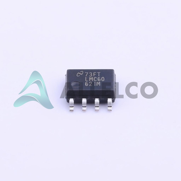
View All

Please refer to the English Version as our Official Version.Return

Europe
France(Français) Germany(Deutsch) Italy(Italia) Russian(русский) Poland(polski) Czech(Čeština) Luxembourg(Lëtzebuergesch) Netherlands(Nederland) Iceland(íslenska) Hungarian(Magyarország) Spain(español) Portugal(Português) Turkey(Türk dili) Bulgaria(Български език) Ukraine(Україна) Greece(Ελλάδα) Israel(עִבְרִית) Sweden(Svenska) Finland(Svenska) Finland(Suomi) Romania(românesc) Moldova(românesc) Slovakia(Slovenská) Denmark(Dansk) Slovenia(Slovenija) Slovenia(Hrvatska) Croatia(Hrvatska) Serbia(Hrvatska) Montenegro(Hrvatska) Bosnia and Herzegovina(Hrvatska) Lithuania(lietuvių) Spain(Português) Switzerland(Deutsch) United Kingdom(English)
Asia/Pacific
Japan(日本語) Korea(한국의) Thailand(ภาษาไทย) Malaysia(Melayu) Singapore(Melayu) Vietnam(Tiếng Việt) Philippines(Pilipino)
Africa, India and Middle East
United Arab Emirates(العربية) Iran(فارسی) Tajikistan(فارسی) India(हिंदी) Madagascar(malaɡasʲ)
South America / Oceania
New Zealand(Maori) Brazil(Português) Angola(Português) Mozambique(Português)
North America
United States(English) Canada(English) Haiti(Ayiti) Mexico(español)
HomeProductsIntegrated Circuits (ICs)Linear - Amplifiers - Instrumentation, OP Amps, Buffer AmpsLMC6062IM
LMC6062IM Image
Image may be representation.
See specifications for product details.
EXPRESS OPTION
Payment method

LMC6062IM - Texas Instruments

Manufacturer Part Number
LMC6062IM
Manufacturer
Texas Instruments
Allelco Part Number
32D-LMC6062IM
Warranty
1 Year Allelco Warranty - Find out more
Stock Status:
19,623 pcs available, New & Original
Parts Description
IC CMOS 2 CIRCUIT 8SOIC
Package
8-SOIC
Data sheet
-
RoHs Status
 
Our certification
In stock: 19623

Required fields are indicated by an asterisk (*)
Please send RFQ, we will respond immediately.

Quantity

Specifications

LMC6062IM Tech Specifications
Texas Instruments - LMC6062IM technical specifications, attributes, parameters and parts with similar specifications to Texas Instruments - LMC6062IM

Product Attribute Attribute Value
Manufacturer Texas Instruments
Voltage - Supply Span (Min) 4.5 V
Voltage - Supply Span (Max) 15.5 V
Voltage - Input Offset 100 µV
Supplier Device Package 8-SOIC
Slew Rate 0.035V/µs
Series LMC®
Package / Case 8-SOIC (0.154", 3.90mm Width)
Package Bulk
Product Attribute Attribute Value
Output Type Push-Pull, Rail-to-Rail
Operating Temperature -40°C ~ 85°C (TJ)
Number of Circuits 2
Mounting Type Surface Mount
Gain Bandwidth Product 100 kHz
Current - Supply 40µA (x2 Channels)
Current - Output / Channel 35 mA
Current - Input Bias 0.01 pA
Amplifier Type CMOS

Environmental & Export Classifications

ATTRIBUTE DESCRIPTION
RoHs Status RoHS non-compliant
Moisture Sensitivity Level (MSL) 1 (Unlimited)
REACH Status REACH Affected
ECCN EAR99

Parts Introduction

LMC6062IM Image
LMC6062IM (1)

Manufacturer Part Number

LMC6062IM

Manufacturer

Texas Instruments

Introduction

Dual operational amplifier (op-amp) integrated circuit (IC)

Product Features and Performance

Rail-to-rail output

Push-pull output stage

100 kHz gain-bandwidth product

Low input bias current of 0.01 pA

Low input offset voltage of 100 μV

Slew rate of 0.035 V/μs

Wide supply voltage range from 4.5 V to 15.5 V

Operates over -40°C to 85°C temperature range

Product Advantages

Versatile op-amp suitable for a wide range of applications

Excellent performance characteristics

Wide operating voltage range

Operates in harsh temperature environments

Key Technical Parameters

2 independent op-amp channels in a single package

8-pin SOIC (Small Outline Integrated Circuit) package

Not RoHS compliant

Quality and Safety Features

Manufactured by a reputable semiconductor company, Texas Instruments

Intended for industrial and commercial applications

Compatibility

Surface mount device

Compatible with standard op-amp applications

Application Areas

Instrumentation and measurement equipment

Industrial process control

Data acquisition systems

General-purpose amplifier circuits

Product Lifecycle

The LMC6062IM is an established op-amp product that is still in production

Replacement or upgrade options may be available from Texas Instruments or other manufacturers

Several Key Reasons to Choose This Product

Excellent performance characteristics, including low input offset voltage, high gain-bandwidth, and low input bias current

Wide operating voltage and temperature range, making it suitable for a variety of applications

Dual op-amp configuration in a single package, providing design flexibility

Manufactured by a reputable semiconductor company, Texas Instruments, ensuring quality and reliability

Availability and ongoing support from the manufacturer

Frequently Asked Questions(FAQ)

How does the LMC6062IM’s input bias current compare to older bipolar op-amps, and what implications does this have for high-impedance sensor interfaces?
The LMC6062IM exhibits an input bias current of just 0.01 pA, which is orders of magnitude lower than typical bipolar op-amps that often exceed 1 nA. This ultra-low leakage enables stable operation in precision applications involving high-value resistors or capacitive loads, such as thermocouple amplifiers or piezoelectric transducers, where stray charge injection could otherwise introduce significant offset drift over time.
What is the practical impact of the LMC6062IM’s rail-to-rail output swing when driving a 10 kΩ load across a ±5 V supply?
With a supply range of ±2.25 V to ±7.75 V (or 4.5 V to 15.5 V single-supply), the LMC6062IM delivers true rail-to-rail output, meaning it can drive voltages within millivolts of the rails even into moderate loads. Driving a 10 kΩ resistor at ±5 V results in minimal voltage drop due to output current capability (35 mA per channel), ensuring full dynamic range without clipping near the power rails—critical for systems requiring maximum signal headroom.
Can the LMC6062IM reliably operate in industrial environments with temperature cycling between -40°C and +85°C?
Yes, the LMC6062IM is specified for junction temperatures from -40°C to +85°C, making it suitable for extended industrial operating conditions. However, performance characteristics such as input offset voltage (100 µV typical) may shift with temperature; designers should account for drift using worst-case values in precision designs or implement calibration routines if required beyond datasheet tolerances.
How does the gain bandwidth product of 100 kHz limit or enable use cases for the LMC6062IM in signal conditioning chains?
At 100 kHz GBW, the LMC6062IM is well-suited for low-frequency analog signal paths such as sensor amplification, audio preamplification, or data acquisition systems sampling below 50 kHz. It would struggle with high-speed feedback loops requiring closed-loop gains above ~10 at frequencies exceeding 10–20 kHz. For such applications, higher GBW devices should be considered unless gain reduction is acceptable.
In what scenarios would the LMC6062IM’s 40 µA total quiescent current per pair present a challenge for battery-powered devices?
While 40 µA total (20 µA per channel) appears modest, in multi-channel battery designs—such as wearable health monitors with multiple physiological sensors—this adds up quickly. Over a year on a 100 mAh coin cell, two channels consume roughly 1.4% of capacity, potentially shortening device life. Designers must weigh this against its rail-to-rail performance and low noise, possibly using shutdown modes if available or switching to lower-power alternatives like the LPV521 series.
How does the LMC6062IM’s slew rate of 0.035 V/µs affect transient response in capacitive load applications?
The 35 mV/µs slew rate limits how fast the output can change under large-signal conditions. When driving capacitive loads (e.g., long cables or filtering capacitors), this can cause slow settling or overshoot during step inputs. For example, a 2 V step takes over 57 µs to settle fully—potentially unacceptable in real-time control loops. Mitigation strategies include adding series resistance at the output or reducing capacitive loading where feasible.
Should the LMC6062IM be used in medical instrumentation given its RoHS non-compliance and REACH status?
The LMC6062IM is RoHS non-compliant and affected by REACH regulations, which restricts its use in certain regulated markets including medical devices sold in the EU. While functionally robust, substitution with modern CMOS equivalents like the TLV9062 or OPA333 may be necessary to meet compliance requirements without sacrificing similar specifications such as input offset voltage or bias current.
What are the implications of the LMC6062IM’s 8-SOIC packaging for thermal management in compact PCB layouts?
As an 8-pin SOIC package (3.9 mm width), the LMC6062IM has limited exposed pad options compared to QFN packages, resulting in higher thermal resistance (~100°C/W). In continuous high-output-current scenarios (e.g., driving LEDs or actuators), self-heating may raise junction temperature above ambient—especially near the 85°C TJ max. Adequate copper pour and airflow become important in sustained-load designs to avoid derating output capability or reliability degradation.
How does the LMC6062IM compare to single-supply alternatives like the LM358 in sensor interface circuits powered from 5 V?
Unlike the LM358—a bipolar amplifier with limited output swing and higher input offset—the LMC6062IM offers rail-to-rail I/O on a single 5 V supply while maintaining sub-pA bias currents and microvolt-level offset. This makes it far superior for precision 5 V sensor frontends like RTDs or photodiodes, where the LM358 would introduce nonlinearities due to output saturation and input-referred errors amplified through high-gain stages.
Is the LMC6062IM suitable for driving ADC input ranges without additional buffering when interfacing to a 12-bit converter?
Provided the ADC input impedance is high enough and the source impedance is low, the LMC6062IM can directly drive most SAR ADCs without buffering. Its 35 mA output drive ensures fast settling into resistive loads, and rail-to-rail swing matches common ADC input spans (e.g., 0–3.3 V). However, for multichannel multiplexed systems, ensure total current draw from the amplifier doesn’t exceed ADC drive capability—especially at conversion rates above 100 ksps, where output slew dominates acquisition time.
What design precautions are needed when cascading multiple LMC6062IM stages to achieve high overall gain?
Cascading multiple LMC6062IM stages increases total noise and cumulative offset errors. Each stage contributes its own input-referred noise (~10–15 nV/√Hz) and offset drift, degrading SNR in low-amplitude signals. Additionally, the 100 kHz GBW constrains usable gain-bandwidth product across stages. A better approach is to use a single high-gain first stage followed by filtering and buffering, minimizing interaction between stages and preserving dynamic range.
How does moisture sensitivity level (MSL) 1 affect handling and shelf-life concerns for the LMC6062IM in production environments?
MSL 1 indicates the LMC6062IM is not susceptible to moisture-induced damage during normal storage and reflow soldering. It can be stored indefinitely at <60% RH and withstand standard Pb-free reflow profiles without baking. This simplifies inventory management and reduces post-reflow failure risks, though standard ESD precautions remain essential due to its CMOS construction.
Can the LMC6062IM safely drive inductive loads such as relays or solenoids in switching applications?
No—the LMC6062IM is not designed for direct drive of inductive loads. Its push-pull output lacks built-in flyback protection, and reverse EMF from relays or solenoids can destroy the internal transistors. External flyback diodes and current-limiting resistors must be added in series with the load, and isolation via optocouplers or MOSFET drivers is recommended to protect the IC.
What role does the LMC6062IM play in precision voltage references or bias networks for ADC drivers?
Due to its extremely low input offset (100 µV max) and bias current (0.01 pA), the LMC6062IM can buffer precision reference voltages with negligible loading error. When configured as a unity-gain follower driving an ADC input, it prevents droop in high-impedance sources like bandgap references, preserving system linearity and accuracy—especially critical in 16-bit+ data converters where 1 LSB corresponds to tens of µV.
How does the LMC6062IM’s dual-circuit architecture benefit instrumentation amplifier topologies compared to single-op-amp solutions?
The dual LMC6062IM provides two independent amplifiers in one package, enabling efficient implementation of differential amplifiers or balanced buffers without increasing board space or parasitics. For instance, building a three-op-amp instrumentation amplifier can use one LMC6062IM as a difference amplifier and another for buffering, improving CMRR and stability over discrete implementations while leveraging matched channel characteristics.
Are there hidden costs or supply chain risks associated with sourcing the LMC6062IM today?
The LMC6062IM is now legacy, with National Semiconductor (now part of Texas Instruments) having discontinued active production. While some distributors still carry stock, lead times are unpredictable and prices have risen significantly. Designers should evaluate newer pin-compatible replacements like the OPA2333 or LPV522 to reduce future obsolescence risk while maintaining comparable performance in low-noise, rail-to-rail applications.

Parts with Similar Specifications

The three parts on the right have similar specifications to Texas Instruments LMC6062IM

Product Attribute LMC6062IMX LMC6062AIMX LMC6062AIM/NOPB LMC6062I MDC
Part Number LMC6062IMX LMC6062AIMX LMC6062AIM/NOPB LMC6062I MDC
Manufacturer Texas Instruments Texas Instruments Texas Instruments Texas Instruments
Operating Temperature - -40°C ~ 85°C 0°C ~ 70°C -40°C ~ 85°C
Package / Case - 196-LFBGA 16-DIP (0.300', 7.62mm) 64-VFQFN Exposed Pad
Output Type - Current - Unbuffered Voltage - Buffered -
Series - - - -
Number of Circuits - - - -
Current - Supply - - - -
Current - Input Bias - - - -
Gain Bandwidth Product - - - -
Package - Tape & Reel (TR) Tube Tape & Reel (TR)
Supplier Device Package - 196-NFBGA (12x12) 16-PDIP 64-VQFN (9x9)
Voltage - Supply Span (Min) - - - -
Voltage - Supply Span (Max) - - - -
Current - Output / Channel - - - -
Slew Rate - - - -
Mounting Type - Surface Mount Through Hole Surface Mount
Voltage - Input Offset - - - -
Amplifier Type - - - -

Customer Reviews

Evaluation: 10 Articles

  • Nath***rooks
    Jun 11, 2026

    Installed this power component in a converter board. Output remained stable under different load conditions and thermal performance was better than expected.

  • Dani***alkerTech
    Jun 1, 2026

    Product works, but setup took more effort than expected. Once configured the MCU ran reliably, although documentation support felt older compared with newer platforms. Fine for maintenance projects.

  • Yuki***aka88
    May 26, 2026

    信号通信プロジェクトでこのRS-485トランシーバーを使用しました。設置は簡単で、長距離ケーブルでも通信は安定していました。消費電力も、以前使用していたものより低くなっています。

  • Stev***aker
    May 20, 2026

    Solid diode for power rectification. Works well in switching circuits.

  • Bran***Lewis
    May 11, 2026

    Compact FPGA with good performance. Suitable for basic signal processing tasks.

  • Oliv***arris
    May 7, 2026

    Reliable I/O expander. Works well in embedded control applications.

  • Jess***Jones
    Apr 17, 2026

    It offers good value for the price, and the specifications match the description. I’ve been using it for two days with no issues, and I’ll definitely buy it again if I need it in the future.

  • Mich***Smith
    Apr 17, 2026

    Shipping was on time, the component pins are neatly aligned, and I tested 10 of them with a multimeter—all readings were within the specified range. Highly recommended.

  • Aman***arris
    Apr 3, 2026

    It was great—the entire process, from placing the order to receiving the package, went very smoothly. The components were consistent, the price was fair, and I had a very pleasant shopping experience.

  • Mike***nch
    Apr 3, 2026

    Better than expected! The resistance and capacitance readings were spot-on, and it passed the test on the first try. The service was reliable, and the packaging was thoughtful—I highly recommend it.

Write a Review

Your Email address will not be published.

Shipment

Delivery Time

In-stock items can be shipped within 24 hours. Some parts will be arranged for delivery within 1-2 days from the date all items arrive at our warehouse. And Allelco ships order once a day at about 17:00, except Sunday. Once the goods are shipped, the estimated delivery time depends on the shipping methods and Delivery destination. The table below shows are the logistic time for some common countries.

Delivery Cost

  1. Use your express account for shipment if you have one.
  2. Use our account for the shipment. Refer to the table below for the approximate charges.
(Different time frame / countries / package size has different price.)

Delivery Method

  1. Global Common Shipment by DHL / UPS / FedEx / TNT / EMS / SF we support.
  2. Others more shipping ways, please get in touch with your customer manager.

Common Countries Logistic Time Reference
Region Country Logistic Time(Day)
America United States 5
Brazil 7
Europe Germany 5
United Kingdom 4
Italy 5
Oceania Australia 6
New Zealand 5
Asia India 4
Japan 4
Middle East Israel 6
DHL & FedEx Shipment Charges Reference
Shipment charges(KG) Reference DHL(USD$)
0.00kg-1.00kg USD$30.00 - USD$60.00
1.00kg-2.00kg USD$40.00 - USD$80.00
2.00kg-3.00kg USD$50.00 - USD$100.00
Note:
The above table is for reference only. There may have some data bias for the uncontrollable factors.
Contact us if you have any questions.
  • QC (Quality Warranty)
  • Payment Support
  • Packaging
  • Certifications & Memberships

QC (Quality Warranty)

Allelco is committed to exceeding customer expectations through customer service excellence, order accuracy, and on-time delivery.
This is achieved through our commitment to the continual improvement of our processes, services, and products.


Strict quality inspection builds a solid foundation for electronic component quality.
  1. Visual inspection
  2. Performance testing and reliability verification
  3. Standardized full-process testing
  4. Precise control of every parameter
We eliminate defective components and ensure the stable operation of electronic devices through professional quality standards.

Payment Support

The payment method can be chosen from the methods shown below: Wire Transfer (T/T, Bank Transfer), Western Union, Credit card, PayPal.
  • HKBea
  • Paypal
  • MasterCard
  • Western-Union
  • VISA
Stable Delivery, Sincere Partnership — Your Faithful Supply Chain Partner
  • Efficient Supply Management
  • Cost-Saving Procurement
  • Fast Sourcing & Delivery
Contact us if you have any questions.

Packaging

Electrostatic Discharge Protection and Handling

All electrostatic-sensitive components are handled in accordance with electrostatic discharge control procedures. The products are hermetically sealed in anti-static safe packaging to prevent electrostatic damage. Appropriate labeling is also applied for identification and traceability. This ensures product integrity during storage, handling and transportation.


ESD

Certifications & Memberships

Third-party certified, strict quality control. Our certification
  • ISO 9001: 2015
  • ISO 13485: 2016
  • ISO 14001: 2015
  • ISO 28000: 2007
  • ISO 45001: 2018
  • GB/T 27922-2011
  • SMTA
  • IPC
  • ESD
  • PSMA
LMC6062IM Image

LMC6062IM

Texas Instruments
32D-LMC6062IM

Want a better price? Add to Cart and Submit RFQ now, we'll contact you immediately.

0 RFQ
Shopping cart (0 Items)
It is empty.
Compare List (0 Items)
It is empty.
Feedback

Your feedback matters! At Allelco, we value the user experience and strive to improve it constantly.
Please share your comments with us via our feedback form, and we'll respond promptly.
Thank you for choosing Allelco.

Subject
E-mail
Comments
Captcha
Drag or click to upload file
Upload File
types: .xls, .xlsx, .doc, .docx, .jpg, .png and .pdf.
Max file size: 10MB