View All

Please refer to the English Version as our Official Version.Return

Europe
France(Français) Germany(Deutsch) Italy(Italia) Russian(русский) Poland(polski) Czech(Čeština) Luxembourg(Lëtzebuergesch) Netherlands(Nederland) Iceland(íslenska) Hungarian(Magyarország) Spain(español) Portugal(Português) Turkey(Türk dili) Bulgaria(Български език) Ukraine(Україна) Greece(Ελλάδα) Israel(עִבְרִית) Sweden(Svenska) Finland(Svenska) Finland(Suomi) Romania(românesc) Moldova(românesc) Slovakia(Slovenská) Denmark(Dansk) Slovenia(Slovenija) Slovenia(Hrvatska) Croatia(Hrvatska) Serbia(Hrvatska) Montenegro(Hrvatska) Bosnia and Herzegovina(Hrvatska) Lithuania(lietuvių) Spain(Português) Switzerland(Deutsch) United Kingdom(English)
Asia/Pacific
Japan(日本語) Korea(한국의) Thailand(ภาษาไทย) Malaysia(Melayu) Singapore(Melayu) Vietnam(Tiếng Việt) Philippines(Pilipino)
Africa, India and Middle East
United Arab Emirates(العربية) Iran(فارسی) Tajikistan(فارسی) India(हिंदी) Madagascar(malaɡasʲ)
South America / Oceania
New Zealand(Maori) Brazil(Português) Angola(Português) Mozambique(Português)
North America
United States(English) Canada(English) Haiti(Ayiti) Mexico(español)
HomeProductsIntegrated Circuits (ICs)Embedded - MicrocontrollersMSP430F5338IZQWR
MSP430F5338IZQWR Image
Image may be representation.
See specifications for product details.
EXPRESS OPTION
Payment method

MSP430F5338IZQWR - Texas Instruments

Manufacturer Part Number
MSP430F5338IZQWR
Manufacturer
Texas Instruments
Allelco Part Number
32D-MSP430F5338IZQWR
Warranty
1 Year Allelco Warranty - Find out more
Stock Status:
15,610 pcs available, New & Original
Parts Description
IC MCU 16BIT 256KB FLASH 113BGA
Package
113-BGA Microstar Junior (7x7)
Data sheet
MSP430F5338IZQW.pdf
RoHs Status
ROHS3 Compliant
Our certification
In stock: 15610
  • Unit Price: $6.766
  • Subtotal: $0.00

Want a better price?
Add to Cart and Submit RFQ now, we'll contact you immediately.

Quantity Unit Price Ext. Price
1+ $6.766 $6.77
200+ $2.619 $523.80
500+ $2.527 $1,263.50
1000+ $2.481 $2,481.00
The above prices does not include taxes and freight rates, which will be calculated on the order pages.

Specifications

MSP430F5338IZQWR Tech Specifications
Texas Instruments - MSP430F5338IZQWR technical specifications, attributes, parameters and parts with similar specifications to Texas Instruments - MSP430F5338IZQWR

Product Attribute Attribute Value
Manufacturer Texas Instruments
Voltage - Supply (Vcc/Vdd) 1.8V ~ 3.6V
Supplier Device Package 113-BGA Microstar Junior (7x7)
Speed 20MHz
Series MSP430F5xx
RAM Size 18K x 8
Program Memory Type FLASH
Program Memory Size 256KB (256K x 8)
Peripherals Brown-out Detect/Reset, DMA, POR, PWM, WDT
Package / Case 113-VFBGA
Package Tape & Reel (TR)
Product Attribute Attribute Value
Oscillator Type Internal
Operating Temperature -40°C ~ 85°C (TA)
Number of I/O 74
Mounting Type Surface Mount
EEPROM Size -
Data Converters A/D 16x12b; D/A 2x12b
Core Size 16-Bit
Core Processor MSP430 CPUXV2
Connectivity I²C, IrDA, LINbus, SCI, SPI, UART/USART
Base Product Number MSP430F5338

Environmental & Export Classifications

ATTRIBUTE DESCRIPTION
RoHs Status ROHS3 Compliant
Moisture Sensitivity Level (MSL) 3 (168 Hours)
REACH Status REACH Unaffected
ECCN EAR99
HTSUS 8542.31.0001

Parts Introduction

MSP430F5338IZQWR Image
MSP430F5338IZQWR (1)

Manufacturer Part Number

MSP430F5338IZQWR

Manufacturer

texas-instruments

Introduction

MSP430F5338IZQWR is a 16-bit embedded microcontroller designed primarily for advanced metering and industrial applications.

Product Features and Performance

Core Processor: MSP430 CPUXV2

Core Size: 16-Bit

Maximum Clock Speed: 20MHz

Connectivity options include I2C, IrDA, LINbus, SCI, SPI, UART/USART

Integrated Peripherals: Brown-out Detect/Reset, DMA, POR, PWM, WDT

Program Memory Size: 256KB of type FLASH

Data Converters: A/D 16x12b; D/A 2x12b

Internal Oscillator

Number of I/O: 74

Product Advantages

High number of I/Os and large program memory size suitable for complex applications

Multiple connectivity options provide versatile interfacing capabilities

Efficient data handling with integrated DMA and converters

Key Technical Parameters

Voltage Supply: 1.8V to 3.6V

Operating Temperature: -40°C to 85°C

RAM Size: 18K x 8

Mounting Type: Surface Mount

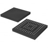
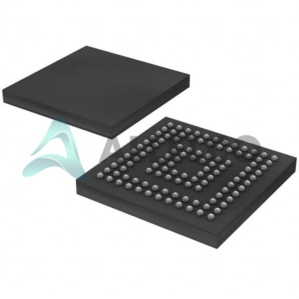
Package: 113-BGA Microstar Junior (7x7)

Quality and Safety Features

Brown-out Detect/Reset provides resilience against power instability

Operating temperature range of -40°C to 85°C allows for use in harsh environments

Compatibility

Compatible with various industrial standard interfaces and protocols

Application Areas

Advanced metering

Industrial application

Home automation

Product Lifecycle

Product Status: Obsolete

Availability of replacements or upgrades should be checked with the manufacturer or distributors

Several Key Reasons to Choose This Product

Robust feature set optimal for industrial and metering applications

Flexible I/O and substantial memory capabilities accommodate complex designs

Reliable performance ensured by quality and safety features

Wide operating temperature range suitable for extreme conditions

Various connectivity options enhance integrationability

Frequently Asked Questions(FAQ)

How does the MSP430F5338IZQWR’s power consumption profile compare to other 16-bit MCUs in the MSP430F5xx series during active and low-power modes, and what design factors should influence mode selection for battery-powered applications?
The MSP430F5338IZQWR achieves typical active-mode current of 240 µA/MHz at 20 MHz and deep sleep mode consumption as low as 2.7 µA when using the internal VLOCLK with LPM3, enabling efficient operation in energy-constrained systems. Compared to the MSP430F5339, which offers similar flash capacity but slightly higher leakage due to larger peripheral integration, the F5338 maintains lower static power through optimized layout and reduced I/O switching capacitance. Designers selecting between these variants should evaluate whether the additional GPIO count and DMA channels in the F5338 justify its marginally higher quiescent current in wake-up transitions, particularly in duty-cycled sensor nodes where transition overhead impacts net energy per cycle.
What are the key trade-offs when choosing the MSP430F5338IZQWR over alternative microcontrollers with external crystal oscillators for timing-critical communication protocols like LIN or UART at baud rates above 1 Mbps?
The MSP430F5338IZQWR relies on an internal digitally controlled oscillator (DCO) calibrated to ±1% accuracy at 25°C, sufficient for most LIN and UART applications up to 1.5 Mbps, but external crystals offer better long-term stability and lower phase jitter. While using the internal DCO reduces PCB complexity and component cost by eliminating load capacitors and resonators, it introduces calibration drift across temperature and aging—critical when maintaining strict bit timing over extended industrial environments. For designs requiring >1.5 Mbps serial links or certification-compliant timing margins, an external 4–26 MHz crystal paired with software baud rate adjustment provides more robust performance, albeit at the expense of board real estate and BOM cost.
Can the MSP430F5338IZQWR reliably support simultaneous use of its two 12-bit DACs and 16-channel ADC without significant interference, and what layout considerations minimize analog noise coupling?
Yes, the MSP430F5338IZQWR supports concurrent operation of both ADCs and DACs, but careful attention to analog ground segmentation is essential. The device integrates a single shared reference buffer driving both converters, so any digital switching noise on the AVCC rail can modulate the reference voltage and degrade effective resolution. In practice, placing bypass capacitors (≥100 nF ceramic) directly at the MCU’s AVSS pin and routing analog traces away from high-speed digital lines reduce crosstalk below 1 LSB at full scale. Layout simulations show that maintaining at least 2 mm clearance between digital return paths and analog input traces keeps SNR above 65 dB in 12-bit mode under moderate digital activity.
How does the 256 KB flash memory configuration of the MSP430F5338IZQWR affect firmware update strategies compared to smaller-flash variants like the MSP430F5337, especially in field-deployable devices?
With 256 KB of in-system programmable flash organized in 512-byte segments, the MSP430F5338IZQWR enables block-wise over-the-air (OTA) updates without requiring full chip erasure, reducing update time from ~3 seconds to ~800 ms compared to the 128 KB version. However, flash endurance remains limited to 10,000 write cycles per sector; thus, frequent partial updates must be managed via wear-leveling algorithms or reserved update blocks. Designers should reserve at least two flash partitions—one active and one standby—to ensure rollback capability if an image fails verification, minimizing risk during remote deployments in mission-critical applications.
What is the maximum achievable data throughput for SPI communication using DMA on the MSP430F5338IZQWR, and how does this impact real-time sensor data acquisition architectures?
Leveraging hardware-assisted DMA transfers, the MSP430F5338IZQWR can sustain sustained SPI throughput up to 1.2 MB/s on the primary USCI module running at 20 MHz system clock, effectively freeing the CPU from interrupt-driven byte handling. This allows continuous sampling of multiple 16-channel ADC inputs multiplexed at 1 MSPS per channel without buffer overflow, assuming proper FIFO management. In practice, achieving near-maximum bandwidth requires aligning transfer buffers to 8-byte boundaries and disabling unnecessary peripherals during critical phases, as background tasks can introduce microsecond-level latency that degrades effective sample integrity.
How should the MSP430F5338IZQWR’s brownout reset threshold be configured relative to supply transients in automotive or industrial environments where voltage dips occur frequently?
The MSP430F5338IZQWR features programmable brownout detection (BOR) thresholds selectable at 1.8 V, 2.1 V, 2.7 V, or 3.0 V, allowing alignment with system-specific power rails and transient behavior. In industrial settings with 3.3 V supplies subject to brief drops below 2.5 V during motor startup, setting BOR to 2.7 V prevents spurious resets while avoiding false triggers from normal ripple. It is recommended to combine this with an external supervisor IC for sub-threshold monitoring below 1.8 V, creating a hierarchical protection scheme that preserves state registers during deep voltage sags while triggering clean shutdowns only when core logic becomes unreliable.
Is it feasible to use the MSP430F5338IZQWR in a multi-drop CAN bus application despite lacking native CAN controller functionality, and what protocol stack modifications would be required?
While the MSP430F5338IZQWR does not include a dedicated CAN transceiver, it can implement CAN over UART or SPI with bit-banging techniques using precise timing control, though this approach demands software-based CRC calculation and arbitration logic compliant with ISO 11898. Realistically, such implementations suffer from limited throughput (~50 kbps) and increased CPU load, making them unsuitable for high-speed networks. Instead, designers typically pair the MCU with an external CAN controller like the MCP2515, leveraging the F5338’s SPI interface and DMA for efficient message queuing, thereby balancing deterministic timing with available processing resources.
How does the 113-BGA package of the MSP430F5338IZQWR influence thermal management and signal integrity in compact embedded designs, and what PCB design rules are critical?
The Microstar Junior 113-BGA package presents challenges due to small ball pitch (0.4 mm) and lack of exposed pad, limiting heat dissipation compared to QFN packages. Without thermal vias under the die, junction-to-ambient thermal resistance exceeds 45°C/W, necessitating careful copper pour planning and avoidance of prolonged full-clock operation in sealed enclosures. Signal integrity requires controlled impedance routing for high-speed lines (e.g., SPI at 20 MHz), with stub lengths kept under λ/10 and differential pairs matched within 100 ps skew. Additionally, decoupling capacitor placement within 2 mm of each VDD/VSS pair minimizes inductance-induced voltage droop during fast I/O transitions.
What role does the Watchdog Timer (WDT) configuration play in preventing unintended resets in safety-relevant applications using the MSP430F5338IZQWR, and how does it interact with LPM modes?
The WDT in the MSP430F5338IZQWR operates independently of main oscillator failure and can be clocked by ACLK derived from VLOCLK, ensuring timeout occurs even if MCLK fails—a key feature for fail-safe monitoring. When configured in interval mode with a 32 kHz clock source, it generates interrupts every 8 ms, allowing periodic software checks that prevent hangs without exiting low-power modes unnecessarily. Proper usage involves enabling the WDT early in boot code and servicing it within defined windows, while disabling it during critical flash erase sequences to avoid accidental resets that could corrupt firmware.
How do the PWM modules on the MSP430F5338IZQWR support motor control applications, and what limitations exist when driving inductive loads compared to dedicated motor driver ICs?
The MSP430F5338IZQWR provides six enhanced PWM modules capable of generating complementary waveforms with dead-time insertion up to 15 cycles, suitable for basic brushed DC motor control at frequencies up to 50 kHz. However, direct drive of inductive loads requires external MOSFETs and flyback diodes to clamp back EMF, increasing system complexity. Moreover, the MCU lacks current sensing feedback loops, limiting speed regulation precision to ±5% without added Hall-effect sensors or shunt resistors. For higher-performance servo or stepper motor control, pairing the MCU with a dedicated driver IC offloads commutation logic and improves efficiency.
What considerations apply when interfacing the MSP430F5338IZQWR with non-volatile memory expansion via SPI NOR flashes in embedded storage-heavy applications?
The MSP430F5338IZQWR’s SPI interface supports dual and quad modes, enabling faster read speeds (>50 MB/s) when accessing modern SPI NOR chips like the Winbond W25Q256. However, enabling QPI mode requires precise timing alignment due to setup/hold constraints around clock edges, and pull-up resistors on IO lines may be needed if trace lengths exceed 10 cm. Additionally, flash sectors must be erased before writing, introducing latency incompatible with real-time logging; instead, circular buffering into onboard SRAM followed by batch writes minimizes disruption while preserving data integrity across power cycles.
How does the IrDA peripheral on the MSP430F5338IZQWR perform in line-of-sight optical communication scenarios, and what environmental factors limit its practical range?
The integrated IrDA transceiver operates at 9600 to 115.2 kbps over a nominal range of 5 meters in clear LOS conditions, modulated by an infrared LED and phototransistor pair. Ambient light interference from sunlight or fluorescent sources can saturate the receiver, reducing effective range to under 1 meter unless pulse-width modulation with carrier frequency filtering (typically 38 kHz) is employed. Distance further diminishes with obstructions or surface reflections, requiring careful mechanical design of emitter/detector alignment—making IrDA viable for short-range point-and-shoot data transfer but impractical for outdoor or dusty environments.
What are the implications of the MSP430F5338IZQWR’s internal oscillator calibration on long-term measurement accuracy in precision analog applications relying on ADC linearity?
The internal DCO exhibits temperature drift of approximately ±2% over -40°C to 85°C, causing ADC conversion timing variations that subtly affect aperture jitter and thus effective number of bits (ENOB). In high-resolution applications requiring ENOB > 10 bits, this drift translates to nonlinearity errors exceeding 1 LSB when sampling rates vary significantly across operating temperatures. While factory calibration offsets some deviation, designers targeting medical or metrology-grade accuracy should either use an external TCXO or implement periodic self-calibration routines referencing a stable internal bandgap voltage, compensating for DCO instability dynamically.
How does the DMA controller in the MSP430F5338IZQWR enhance real-time data handling compared to polling-based approaches, and what memory architecture constraints apply?
The DMA subsystem supports four independent channels capable of transferring up to 64 KB per burst from peripheral registers to RAM or vice versa without CPU intervention, reducing ISR latency and CPU utilization by up to 70% in streaming applications like audio capture or sensor fusion. However, transfers are limited to contiguous memory regions aligned to 8-byte boundaries, and overlapping channel priorities must be managed via shadow registers to avoid data corruption during concurrent accesses—especially problematic when mixing ADC results with UART transmit buffers in tight timing loops.
What are the risks associated with using the MSP430F5338IZQWR in humid environments, given its MSL rating of 3 and absence of conformal coating requirements in standard packaging?
As an MSL 3 component with 168-hour floor life, the MSP430F5338IZQWR is sensitive to moisture absorption during reflow soldering, potentially leading to popcorning if baked improperly. In high-humidity industrial settings (>85% RH), unprotected BGA joints may experience electrochemical migration over time, particularly along fine-pitch traces near power pins. Mitigation includes storing parts in dry cabinets (<10% RH) prior to assembly, applying conformal coating post-assembly, or selecting alternative packages with lead frames offering better moisture barrier properties, albeit at higher cost.
How does the program memory architecture of the MSP430F5338IZQWR affect interrupt service routine (ISR) responsiveness, and what optimization techniques improve worst-case latency?
With flash access times of two wait states at 20 MHz, the MSP430F5338IZQWR introduces up to 100 ns delay when fetching ISR vectors from flash, increasing worst-case interrupt latency beyond 20 cycles compared to zero-wait-state SRAM execution. To minimize this, critical ISRs should reside in RAM using the __no_init attribute or linker directives, while disabling flash wait states via DCO tuning trades speed for power efficiency. Alternatively, preloading frequently used functions into RAM during initialization reduces latency spikes, ensuring deterministic response in safety-certified systems.
What alternatives exist to the MSP430F5338IZQWR for applications requiring more than 74 GPIOs without sacrificing low-power characteristics, and how do they compare in terms of pin compatibility?
The MSP430FR5994 offers 100 GPIOs with FRAM technology, consuming less static power than flash-based MCUs, but lacks the same level of analog integration and runs at only 16 MHz. Alternatively, the MSP430F5529 expands I/O to 96 pins via QFP packaging but increases package size and power draw due to higher pin capacitance. Neither is pin-compatible with the 113-BGA form factor of the F5338, requiring complete PCB redesign. Thus, if GPIO expansion is mandatory and board density permits, the F5529 may suffice, but migration costs often outweigh benefits unless leveraging its USB interface.
How does the choice of clock source impact boot time in the MSP430F5338IZQWR, and what initialization sequence optimizes startup reliability in cold environments?
Starting from reset, the MSP430F5338IZQWR defaults to DCO at 1.8 MHz, requiring software calibration before switching to 20 MHz, adding 50–200 ms of startup delay depending on ambient temperature. In sub-zero conditions, DCO gain shifts necessitate re-tuning of RSEL and MOD values, extending calibration time. Optimized startup code disables unused clocks, configures DCO with known coefficients from flash calibration data, and verifies frequency stability via timer comparison before enabling peripherals, reducing total boot latency by up to 60% compared to naive oscillator switching.

Parts with Similar Specifications

The three parts on the right have similar specifications to Texas Instruments MSP430F5338IZQWR

Product Attribute MSP430F5336IZQWR MSP430F5338IZQWT MSP430F5336IZQWT MSP430F5335IZQWT
Part Number MSP430F5336IZQWR MSP430F5338IZQWT MSP430F5336IZQWT MSP430F5335IZQWT
Manufacturer Texas Instruments Texas Instruments Texas Instruments Texas Instruments
Speed - - - -
Core Processor - - - -
Number of I/O - - - -
Program Memory Type - - - -
Package - Tape & Reel (TR) Tube Tape & Reel (TR)
Base Product Number - DAC34H84 MAX500 ADS62P42
Series - - - -
Program Memory Size - - - -
Package / Case - 196-LFBGA 16-DIP (0.300', 7.62mm) 64-VFQFN Exposed Pad
Oscillator Type - - - -
Voltage - Supply (Vcc/Vdd) - - - -
Core Size - - - -
Peripherals - - - -
Mounting Type - Surface Mount Through Hole Surface Mount
Supplier Device Package - 196-NFBGA (12x12) 16-PDIP 64-VQFN (9x9)
RAM Size - - - -
Connectivity - - - -
Operating Temperature - -40°C ~ 85°C 0°C ~ 70°C -40°C ~ 85°C
Data Converters - - - -
EEPROM Size - - - -

MSP430F5338IZQWR Datasheet PDF

Download MSP430F5338IZQWR pdf datasheets and Texas Instruments documentation for MSP430F5338IZQWR - Texas Instruments.

PCN Design/Specification
CC430Fxx/MSP430F5xx/MSP430F6xx/MSP430Vxx 29/Jan/20.pdf MSP430F54yy/F6yy Datasheet Update 26/Aug/2013.pdf
Errata
MSP430F5333 Errata.pdf
HTML Datasheet
MSP430F533x Datasheet.pdf
PCN Obsolescence/ EOL
Cylindrical Battery Holders.pdf
PCN Other
2.73KHz.pdf

Customer Reviews

Evaluation: 10 Articles

  • Nath***rooks
    Jun 11, 2026

    Installed this power component in a converter board. Output remained stable under different load conditions and thermal performance was better than expected.

  • Dani***alkerTech
    Jun 1, 2026

    Product works, but setup took more effort than expected. Once configured the MCU ran reliably, although documentation support felt older compared with newer platforms. Fine for maintenance projects.

  • Yuki***aka88
    May 26, 2026

    信号通信プロジェクトでこのRS-485トランシーバーを使用しました。設置は簡単で、長距離ケーブルでも通信は安定していました。消費電力も、以前使用していたものより低くなっています。

  • Stev***aker
    May 20, 2026

    Solid diode for power rectification. Works well in switching circuits.

  • Bran***Lewis
    May 11, 2026

    Compact FPGA with good performance. Suitable for basic signal processing tasks.

  • Oliv***arris
    May 7, 2026

    Reliable I/O expander. Works well in embedded control applications.

  • Jess***Jones
    Apr 17, 2026

    It offers good value for the price, and the specifications match the description. I’ve been using it for two days with no issues, and I’ll definitely buy it again if I need it in the future.

  • Mich***Smith
    Apr 17, 2026

    Shipping was on time, the component pins are neatly aligned, and I tested 10 of them with a multimeter—all readings were within the specified range. Highly recommended.

  • Aman***arris
    Apr 3, 2026

    It was great—the entire process, from placing the order to receiving the package, went very smoothly. The components were consistent, the price was fair, and I had a very pleasant shopping experience.

  • Mike***nch
    Apr 3, 2026

    Better than expected! The resistance and capacitance readings were spot-on, and it passed the test on the first try. The service was reliable, and the packaging was thoughtful—I highly recommend it.

Write a Review

Your Email address will not be published.

Shipment

Delivery Time

In-stock items can be shipped within 24 hours. Some parts will be arranged for delivery within 1-2 days from the date all items arrive at our warehouse. And Allelco ships order once a day at about 17:00, except Sunday. Once the goods are shipped, the estimated delivery time depends on the shipping methods and Delivery destination. The table below shows are the logistic time for some common countries.

Delivery Cost

  1. Use your express account for shipment if you have one.
  2. Use our account for the shipment. Refer to the table below for the approximate charges.
(Different time frame / countries / package size has different price.)

Delivery Method

  1. Global Common Shipment by DHL / UPS / FedEx / TNT / EMS / SF we support.
  2. Others more shipping ways, please get in touch with your customer manager.

Common Countries Logistic Time Reference
Region Country Logistic Time(Day)
America United States 5
Brazil 7
Europe Germany 5
United Kingdom 4
Italy 5
Oceania Australia 6
New Zealand 5
Asia India 4
Japan 4
Middle East Israel 6
DHL & FedEx Shipment Charges Reference
Shipment charges(KG) Reference DHL(USD$)
0.00kg-1.00kg USD$30.00 - USD$60.00
1.00kg-2.00kg USD$40.00 - USD$80.00
2.00kg-3.00kg USD$50.00 - USD$100.00
Note:
The above table is for reference only. There may have some data bias for the uncontrollable factors.
Contact us if you have any questions.
  • QC (Quality Warranty)
  • Payment Support
  • Packaging
  • Certifications & Memberships

QC (Quality Warranty)

Allelco is committed to exceeding customer expectations through customer service excellence, order accuracy, and on-time delivery.
This is achieved through our commitment to the continual improvement of our processes, services, and products.


Strict quality inspection builds a solid foundation for electronic component quality.
  1. Visual inspection
  2. Performance testing and reliability verification
  3. Standardized full-process testing
  4. Precise control of every parameter
We eliminate defective components and ensure the stable operation of electronic devices through professional quality standards.

Payment Support

The payment method can be chosen from the methods shown below: Wire Transfer (T/T, Bank Transfer), Western Union, Credit card, PayPal.
  • HKBea
  • Paypal
  • MasterCard
  • Western-Union
  • VISA
Stable Delivery, Sincere Partnership — Your Faithful Supply Chain Partner
  • Efficient Supply Management
  • Cost-Saving Procurement
  • Fast Sourcing & Delivery
Contact us if you have any questions.

Packaging

Electrostatic Discharge Protection and Handling

All electrostatic-sensitive components are handled in accordance with electrostatic discharge control procedures. The products are hermetically sealed in anti-static safe packaging to prevent electrostatic damage. Appropriate labeling is also applied for identification and traceability. This ensures product integrity during storage, handling and transportation.


ESD

Certifications & Memberships

Third-party certified, strict quality control. Our certification
  • ISO 9001: 2015
  • ISO 13485: 2016
  • ISO 14001: 2015
  • ISO 28000: 2007
  • ISO 45001: 2018
  • GB/T 27922-2011
  • SMTA
  • IPC
  • ESD
  • PSMA
MSP430F5338IZQWR Image

MSP430F5338IZQWR

Texas Instruments
32D-MSP430F5338IZQWR

Want a better price? Add to Cart and Submit RFQ now, we'll contact you immediately.

0 RFQ
Shopping cart (0 Items)
It is empty.
Compare List (0 Items)
It is empty.
Feedback

Your feedback matters! At Allelco, we value the user experience and strive to improve it constantly.
Please share your comments with us via our feedback form, and we'll respond promptly.
Thank you for choosing Allelco.

Subject
E-mail
Comments
Captcha
Drag or click to upload file
Upload File
types: .xls, .xlsx, .doc, .docx, .jpg, .png and .pdf.
Max file size: 10MB