View All

Please refer to the English Version as our Official Version.Return

Europe
France(Français) Germany(Deutsch) Italy(Italia) Russian(русский) Poland(polski) Czech(Čeština) Luxembourg(Lëtzebuergesch) Netherlands(Nederland) Iceland(íslenska) Hungarian(Magyarország) Spain(español) Portugal(Português) Turkey(Türk dili) Bulgaria(Български език) Ukraine(Україна) Greece(Ελλάδα) Israel(עִבְרִית) Sweden(Svenska) Finland(Svenska) Finland(Suomi) Romania(românesc) Moldova(românesc) Slovakia(Slovenská) Denmark(Dansk) Slovenia(Slovenija) Slovenia(Hrvatska) Croatia(Hrvatska) Serbia(Hrvatska) Montenegro(Hrvatska) Bosnia and Herzegovina(Hrvatska) Lithuania(lietuvių) Spain(Português) Switzerland(Deutsch) United Kingdom(English)
Asia/Pacific
Japan(日本語) Korea(한국의) Thailand(ภาษาไทย) Malaysia(Melayu) Singapore(Melayu) Vietnam(Tiếng Việt) Philippines(Pilipino)
Africa, India and Middle East
United Arab Emirates(العربية) Iran(فارسی) Tajikistan(فارسی) India(हिंदी) Madagascar(malaɡasʲ)
South America / Oceania
New Zealand(Maori) Brazil(Português) Angola(Português) Mozambique(Português)
North America
United States(English) Canada(English) Haiti(Ayiti) Mexico(español)
HomeProductsIntegrated Circuits (ICs)Linear - Amplifiers - Instrumentation, OP Amps, Buffer AmpsOPA4132UA/2K5
OPA4132UA/2K5 Image
Image may be representation.
See specifications for product details.
EXPRESS OPTION
Payment method

OPA4132UA/2K5 - Texas Instruments

Manufacturer Part Number
OPA4132UA/2K5
Manufacturer
Texas Instruments
Allelco Part Number
32D-OPA4132UA/2K5
Warranty
1 Year Allelco Warranty - Find out more
Stock Status:
5,490 pcs available, New & Original
Parts Description
IC OPAMP JFET 4 CIRCUIT 14SOIC
Package
14-SOIC
Data sheet
-
RoHs Status
ROHS3 Compliant
Our certification
In stock: 5490
  • Unit Price: $6.813
  • Subtotal: $0.00

Want a better price?
Add to Cart and Submit RFQ now, we'll contact you immediately.

Quantity Unit Price Ext. Price
1+ $6.813 $6.81
10+ $5.977 $59.77
30+ $5.467 $164.01
100+ $5.04 $504.00
The above prices does not include taxes and freight rates, which will be calculated on the order pages.

Specifications

OPA4132UA/2K5 Tech Specifications
Texas Instruments - OPA4132UA/2K5 technical specifications, attributes, parameters and parts with similar specifications to Texas Instruments - OPA4132UA/2K5

Product Attribute Attribute Value
Manufacturer Texas Instruments
Voltage - Supply Span (Min) 5 V
Voltage - Supply Span (Max) 36 V
Voltage - Input Offset 500 µV
Supplier Device Package 14-SOIC
Slew Rate 20V/µs
Series OPAx132
Package / Case 14-SOIC (0.154", 3.90mm Width)
Package Tape & Reel (TR)
Output Type -
Product Attribute Attribute Value
Operating Temperature -40°C ~ 85°C
Number of Circuits 4
Mounting Type Surface Mount
Gain Bandwidth Product 8 MHz
Current - Supply 4mA (x4 Channels)
Current - Output / Channel 40 mA
Current - Input Bias 5 pA
Base Product Number OPA4132
Amplifier Type J-FET

Environmental & Export Classifications

ATTRIBUTE DESCRIPTION
RoHs Status ROHS3 Compliant
Moisture Sensitivity Level (MSL) 3 (168 Hours)
REACH Status REACH Unaffected
ECCN EAR99

Parts Introduction

OPA4132UA/2K5 Image
OPA4132UA/2K5 (1)

Manufacturer Part Number

OPA4132UA/2K5

Manufacturer

Texas Instruments

Introduction

Quad, low-noise, JFET-input operational amplifier

Product Features and Performance

Quad operational amplifier

Low-noise performance

JFET-input

Wide supply voltage range of 5V to 36V

High output current drive of 40mA per channel

Low input bias current of 5pA

High slew rate of 20V/µs

Low input offset voltage of 500μV

Wide gain bandwidth of 8MHz

4 independent amplifier channels

Product Advantages

Excellent noise and offset performance for precision applications

High output drive capability suitable for driving large capacitive loads

Wide supply voltage range for versatile use in various systems

Compact 14-SOIC package saves board space

Key Technical Parameters

Gain bandwidth product: 8MHz

Supply voltage range: 5V to 36V

Output current per channel: 40mA

Input offset voltage: 500μV

Input bias current: 5pA

Slew rate: 20V/μs

Quality and Safety Features

RoHS3 compliant

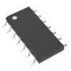
14-SOIC surface mount package

Compatibility

Suitable for a wide range of instrumentation, measurement, and control applications

Application Areas

Precision analog circuits

Industrial and medical instrumentation

Sensor conditioning

Data acquisition systems

General-purpose amplification

Product Lifecycle

Current product, no discontinuation planned

Replacements and upgrades available within the OPAx132 series

Several Key Reasons to Choose This Product

Excellent noise and offset performance for high-precision applications

High output drive capability for driving capacitive loads

Wide supply voltage range for versatile system integration

Compact 14-SOIC package for space-constrained designs

Established Texas Instruments quality and reliability

Frequently Asked Questions(FAQ)

What are the key electrical characteristics of the OPA4132UA/2K5 that make it suitable for precision analog signal conditioning in industrial sensor interfaces?
The OPA4132UA/2K5 features a low input bias current of 5 pA, which minimizes loading effects on high-impedance sensor outputs such as piezoelectric or capacitive transducers. Its input offset voltage of 500 µV enables accurate amplification of small differential signals without significant DC error, critical in bridge-based sensors like strain gauges or thermocouples. With a gain bandwidth product of 8 MHz and slew rate of 20 V/µs, it maintains dynamic performance across a wide frequency range while delivering 40 mA output drive per channel—sufficient for driving ADC inputs or buffering long traces in noisy environments.
How does the supply voltage range of the OPA4132UA/2K5 influence its selection over rail-to-rail op-amps when designing battery-powered data acquisition systems?
Unlike rail-to-rail output stages that may introduce distortion near supply rails, the OPA4132UA/2K5 operates from ±2.5 V to ±18 V (single-supply 5 V to 36 V), offering stable performance across a broad span without requiring precise headroom management. In a 12 V battery system with expected voltage sag down to 9 V, this device avoids the complexity of level-shifting circuits required by some rail-to-rail alternatives. However, designers must ensure signal swings remain within non-inverting input and linear output limits to prevent compression, especially given its J-FET input stage’s limited common-mode range at lower supplies.
Can the OPA4132UA/2K5 reliably interface with 3.3 V microcontrollers when powered from a 5 V logic rail, and what layout considerations are necessary?
Yes, but only if the op-amp’s output swing is constrained below the microcontroller’s VIL threshold. At 5 V supply, the OPA4132UA/2K5 typically provides 30 mV output headroom, yielding an effective output high near 4.97 V—well above 3.3 V CMOS logic thresholds. However, noise margins degrade compared to native 3.3 V designs. A practical approach uses the op-amp to buffer analog signals before digitization, then employs digital isolation or level translation only where digital lines cross domains. PCB layout must minimize parasitic coupling between analog and digital grounds, using a star ground tied at the power entry point to avoid ground loops.
How should thermal derating be applied when operating the OPA4132UA/2K5 in continuous full-load conditions within an enclosed industrial enclosure?
With a total quiescent current of 4 mA across all four channels and maximum output current per channel of 40 mA, power dissipation depends heavily on output swing and load impedance. For example, driving a 100 Ω load at peak output (say 20 mA × 100 Ω = 2 mW per channel) results in minimal heating. However, in unity-gain buffer configurations with capacitive loads >1 nF, stability may require series resistance, increasing resistive losses. Assuming θJA = 100°C/W for standard SOIC on FR4, a 100 mW dissipation could raise junction temperature by 10°C above ambient. In sealed enclosures with poor airflow, derate allowable output current or add ventilation to maintain Tj < 125°C under worst-case conditions.
Why might someone choose dual-supply operation with the OPA4132UA/2K5 instead of single-supply for ECG monitoring applications?
ECG signals are inherently bipolar, centered around zero volts. Using dual supplies (±5 V) allows the OPA4132UA/2K5 to handle negative-going excursions without clipping, preserving waveform integrity. In single-supply designs, DC biasing introduces additional circuitry that can amplify electrode offset potentials and increase motion artifact susceptibility. The J-FET input stage’s high input impedance (>10¹² Ω) ensures minimal charge injection into the patient, provided guard rings and proper shielding are implemented. Dual-supply also simplifies anti-aliasing filter design since the full Nyquist band remains symmetric about zero.
What is the impact of the OPA4132UA/2K5’s J-FET input architecture on EMI susceptibility in motor control feedback loops?
J-FET inputs exhibit higher gate leakage than bipolar transistors but benefit from inherent Miller capacitance reduction due to absence of base-width modulation. In environments with fast dI/dt transients from PWM motors, the op-amp’s 5 pA bias current implies negligible transient currents through input protection diodes, reducing latch-up risk. However, without integrated ESD diodes (as found in newer CMOS op-amps), external protection networks must clamp voltages to within VDD–VSS. Layout proximity to motor leads should include ferrite beads, RC snubbers, and partitioned ground planes to limit coupled noise into sensitive input nodes.
How does the gain bandwidth product versus slew rate trade-off manifest in video preamplifier applications using the OPA4132UA/2K5?
For composite video signals (~5 MHz bandwidth), the OPA4132UA/2K5’s 8 MHz GBW supports closed-loop gains up to approximately 1.6 without peaking, assuming dominant-pole compensation. However, large output transitions (e.g., sync pulses) require sufficient slew rate—20 V/µs here translates to a maximum undistorted ramp rate of 20 V/µs. A 1 V step takes 50 ns to settle, potentially causing overshoot if feedback network delays exceed this. Thus, while usable for NTSC/PAL decoding stages, higher-resolution video may demand wider bandwidth or slew-enhanced architectures, limiting utility in HDMI front-end buffers.
What precautions are needed when cascading multiple OPA4132UA/2K5 stages in active filter banks for audio equalization?
Each stage introduces phase shift that accumulates across frequencies. At 20 kHz, with 8 MHz GBW and typical second-order topology, group delay can exceed 200 ns per section. Cascading three such filters risks instability unless inter-stage isolation is enforced via buffering or reduced Q factors. Additionally, cumulative input offset (up to 500 µV × gain product) must be compensated, either through null pins or AC coupling. Power sequencing matters less due to low quiescent current, but decoupling each supply pin with 100 nF ceramic capacitors close to the package prevents crosstalk between channels, preserving THD+N below 0.01% in stereo configurations.
How does the OPA4132UA/2K5 compare to CMOS alternatives like the OPA4340 in terms of input bias current and settling time for photodiode transimpedance amplifiers?
The OPA4132UA/2K5’s 5 pA input bias current is two orders of magnitude lower than typical CMOS op-amps like the OPA4340 (which may have 500 pA), making it preferable for detecting sub-picoampere photocurrents from avalanche photodiodes. However, CMOS devices often achieve faster settling times (e.g., 50 ns vs. ~100 ns for OPA4132UA/2K5 at 12-bit accuracy) due to higher slew rates and optimized internal compensation. When using the OPA4132UA/2K5, ensure compensation capacitor values balance bandwidth against stability, especially with large feedback resistors (>1 MΩ), to avoid peaking that degrades pulse response in pulsed laser detection systems.
Is the OPA4132UA/2K5 appropriate for driving relay coils in switching power supply control loops, and what external components are essential?
While the op-amp can source up to 40 mA per channel, relay coils often draw hundreds of mA during pull-in. Thus, the OPA4132UA/2K5 should drive a MOSFET or transistor stage rather than directly switch the coil. If used for sensing feedback (e.g., current sense across coil), its low offset voltage ensures accurate turn-on/off thresholds. However, inductive kickback demands flyback diodes across the coil or TVS protection at the op-amp output if switching occurs near supply rails. Thermal stress is minimal unless continuously switching at high duty cycles, so heatsinking is generally unnecessary in this configuration.
What role does the moisture sensitivity level (MSL 3) play in the handling and storage of OPA4132UA/2K5 units delivered in tape-and-reel format?
MSL 3 indicates the OPA4132UA/2K5 can withstand 168 hours of exposure to 60°C/60% RH before soldering risks arise. Beyond this, popcorning may occur during reflow, damaging bond wires. In automated assembly lines, desiccant-sealed dry packs and humidity indicators are mandatory. After unpacking, components should be used within the 168-hour window or baked at 125°C for 24 hours if stored beyond that period. This applies regardless of packaging type, including the TR (tape & reel) format specified for the OPA4132UA/2K5.
How does the operating temperature range (-40°C to 85°C) affect drift parameters in precision measurement systems using the OPA4132UA/2K5 over time?
Over the full -40°C to 85°C range, input offset voltage can drift up to ±2.5 mV (typical), though datasheet specifies initial offset of 500 µV. This variation necessitates calibration in high-accuracy systems or use of chopper-stabilized alternatives if sub-millivolt precision is required without trimming. Temperature coefficient of offset voltage (TC_VOS) is not guaranteed but historically tracks around 5 µV/°C for J-FET devices. Designers should allocate margin in gain error budgets and consider periodic recalibration cycles, especially in unattended field deployments where environmental cycling occurs frequently.
Can the OPA4132UA/2K5 operate reliably in automotive-grade environments despite being specified only up to 85°C?
No. Automotive applications require qualification to AEC-Q100 Grade 2 (–40°C to +125°C) or Grade 1 (+150°C). Since the OPA4132UA/2K5 lacks such certification, it is unsuitable for direct deployment in engine compartments or lighting systems subject to prolonged high temperatures. However, it may be acceptable in body electronics (e.g., seat controls) where ambient temps rarely exceed 85°C, provided thermal management maintains junction temperature within limits. Always verify actual case temperatures under worst-case load profiles before declaring compliance.
What is the significance of the 14-SOIC package dimensions (0.154", 3.90mm width) in relation to PCB real estate and routing density?
The 14-pin SOIC footprint occupies approximately 8.6 mm length × 4.9 mm width, fitting standard 0.1" grid patterns. Its narrow profile allows dense stacking in multi-layer boards but limits access to unused pins during prototyping. The exposed pad (if present) enhances thermal conduction but requires proper solder fillets to avoid voids. Given the OPA4132UA/2K5’s moderate power dissipation (<200 mW typical), thermal vias under the package are optional but recommended for reliability in extended operation near temperature extremes. Routing adjacent analog signals away from digital nets helps preserve SNR in mixed-signal designs.
How does the RoHS3 compliance status of the OPA4132UA/2K5 affect global market eligibility, particularly in China and the EU?
RoHS3 compliance means the OPA4132UA/2K5 meets Directive 2015/863/EU, restricting lead, mercury, cadmium, hexavalent chromium, PBB, PBDE, DEHP, BBP, and DIBP. This ensures market access across Europe, North America, and most of Asia except China, which follows its own GB standards with slightly different exemptions. However, since the OPA4132UA/2K5 contains no restricted substances above thresholds, it satisfies both regimes. Suppliers must provide full material declarations (IMDS or similar) upon request for supply chain traceability.
What precautions should be taken during reflow soldering when mounting the OPA4132UA/2K5 on lead-free PCBs?
Standard JEDEC J-STD-020D profiles apply: peak reflow temperature ≤260°C, dwell time ≤60 seconds. The OPA4132UA/2K5 has an absolute maximum junction temperature of 150°C, so with typical θJA ≈ 100°C/W, sustained power dissipation must be kept below 100 mW during reflow to avoid thermal overload. Avoid localized hot spots; uniform heating minimizes stress on internal die attach. Post-reflow inspection should check for tombstoning or insufficient wetting, especially on fine-pitch pads common in 14-pin SOIC layouts.

Parts with Similar Specifications

The three parts on the right have similar specifications to Texas Instruments OPA4132UA/2K5

Product Attribute OPA4132UA/2K5E4 OPA4132UA/2K5G4 OPA4134UA/2K5 OPA4134UA/2K5E4
Part Number OPA4132UA/2K5E4 OPA4132UA/2K5G4 OPA4134UA/2K5 OPA4134UA/2K5E4
Manufacturer Luminary Micro / Texas Instruments Texas Instruments Texas Instruments Texas Instruments
Series - - - -
Current - Input Bias - - - -
Number of Circuits - - - -
Package / Case - 196-LFBGA 16-DIP (0.300', 7.62mm) 64-VFQFN Exposed Pad
Current - Supply - - - -
Slew Rate - - - -
Mounting Type - Surface Mount Through Hole Surface Mount
Output Type - Current - Unbuffered Voltage - Buffered -
Voltage - Input Offset - - - -
Package - Tape & Reel (TR) Tube Tape & Reel (TR)
Voltage - Supply Span (Max) - - - -
Current - Output / Channel - - - -
Amplifier Type - - - -
Base Product Number - DAC34H84 MAX500 ADS62P42
Voltage - Supply Span (Min) - - - -
Gain Bandwidth Product - - - -
Operating Temperature - -40°C ~ 85°C 0°C ~ 70°C -40°C ~ 85°C
Supplier Device Package - 196-NFBGA (12x12) 16-PDIP 64-VQFN (9x9)

Customer Reviews

Evaluation: 10 Articles

  • Nath***rooks
    Jun 11, 2026

    Installed this power component in a converter board. Output remained stable under different load conditions and thermal performance was better than expected.

  • Dani***alkerTech
    Jun 1, 2026

    Product works, but setup took more effort than expected. Once configured the MCU ran reliably, although documentation support felt older compared with newer platforms. Fine for maintenance projects.

  • Yuki***aka88
    May 26, 2026

    信号通信プロジェクトでこのRS-485トランシーバーを使用しました。設置は簡単で、長距離ケーブルでも通信は安定していました。消費電力も、以前使用していたものより低くなっています。

  • Stev***aker
    May 20, 2026

    Solid diode for power rectification. Works well in switching circuits.

  • Bran***Lewis
    May 11, 2026

    Compact FPGA with good performance. Suitable for basic signal processing tasks.

  • Oliv***arris
    May 7, 2026

    Reliable I/O expander. Works well in embedded control applications.

  • Jess***Jones
    Apr 17, 2026

    It offers good value for the price, and the specifications match the description. I’ve been using it for two days with no issues, and I’ll definitely buy it again if I need it in the future.

  • Mich***Smith
    Apr 17, 2026

    Shipping was on time, the component pins are neatly aligned, and I tested 10 of them with a multimeter—all readings were within the specified range. Highly recommended.

  • Aman***arris
    Apr 3, 2026

    It was great—the entire process, from placing the order to receiving the package, went very smoothly. The components were consistent, the price was fair, and I had a very pleasant shopping experience.

  • Mike***nch
    Apr 3, 2026

    Better than expected! The resistance and capacitance readings were spot-on, and it passed the test on the first try. The service was reliable, and the packaging was thoughtful—I highly recommend it.

Write a Review

Your Email address will not be published.

Shipment

Delivery Time

In-stock items can be shipped within 24 hours. Some parts will be arranged for delivery within 1-2 days from the date all items arrive at our warehouse. And Allelco ships order once a day at about 17:00, except Sunday. Once the goods are shipped, the estimated delivery time depends on the shipping methods and Delivery destination. The table below shows are the logistic time for some common countries.

Delivery Cost

  1. Use your express account for shipment if you have one.
  2. Use our account for the shipment. Refer to the table below for the approximate charges.
(Different time frame / countries / package size has different price.)

Delivery Method

  1. Global Common Shipment by DHL / UPS / FedEx / TNT / EMS / SF we support.
  2. Others more shipping ways, please get in touch with your customer manager.

Common Countries Logistic Time Reference
Region Country Logistic Time(Day)
America United States 5
Brazil 7
Europe Germany 5
United Kingdom 4
Italy 5
Oceania Australia 6
New Zealand 5
Asia India 4
Japan 4
Middle East Israel 6
DHL & FedEx Shipment Charges Reference
Shipment charges(KG) Reference DHL(USD$)
0.00kg-1.00kg USD$30.00 - USD$60.00
1.00kg-2.00kg USD$40.00 - USD$80.00
2.00kg-3.00kg USD$50.00 - USD$100.00
Note:
The above table is for reference only. There may have some data bias for the uncontrollable factors.
Contact us if you have any questions.
  • QC (Quality Warranty)
  • Payment Support
  • Packaging
  • Certifications & Memberships

QC (Quality Warranty)

Allelco is committed to exceeding customer expectations through customer service excellence, order accuracy, and on-time delivery.
This is achieved through our commitment to the continual improvement of our processes, services, and products.


Strict quality inspection builds a solid foundation for electronic component quality.
  1. Visual inspection
  2. Performance testing and reliability verification
  3. Standardized full-process testing
  4. Precise control of every parameter
We eliminate defective components and ensure the stable operation of electronic devices through professional quality standards.

Payment Support

The payment method can be chosen from the methods shown below: Wire Transfer (T/T, Bank Transfer), Western Union, Credit card, PayPal.
  • HKBea
  • Paypal
  • MasterCard
  • Western-Union
  • VISA
Stable Delivery, Sincere Partnership — Your Faithful Supply Chain Partner
  • Efficient Supply Management
  • Cost-Saving Procurement
  • Fast Sourcing & Delivery
Contact us if you have any questions.

Packaging

Electrostatic Discharge Protection and Handling

All electrostatic-sensitive components are handled in accordance with electrostatic discharge control procedures. The products are hermetically sealed in anti-static safe packaging to prevent electrostatic damage. Appropriate labeling is also applied for identification and traceability. This ensures product integrity during storage, handling and transportation.


ESD

Certifications & Memberships

Third-party certified, strict quality control. Our certification
  • ISO 9001: 2015
  • ISO 13485: 2016
  • ISO 14001: 2015
  • ISO 28000: 2007
  • ISO 45001: 2018
  • GB/T 27922-2011
  • SMTA
  • IPC
  • ESD
  • PSMA
OPA4132UA/2K5 Image

OPA4132UA/2K5

Texas Instruments
32D-OPA4132UA/2K5

Want a better price? Add to Cart and Submit RFQ now, we'll contact you immediately.

0 RFQ
Shopping cart (0 Items)
It is empty.
Compare List (0 Items)
It is empty.
Feedback

Your feedback matters! At Allelco, we value the user experience and strive to improve it constantly.
Please share your comments with us via our feedback form, and we'll respond promptly.
Thank you for choosing Allelco.

Subject
E-mail
Comments
Captcha
Drag or click to upload file
Upload File
types: .xls, .xlsx, .doc, .docx, .jpg, .png and .pdf.
Max file size: 10MB