View All

Please refer to the English Version as our Official Version.Return

Europe
France(Français) Germany(Deutsch) Italy(Italia) Russian(русский) Poland(polski) Czech(Čeština) Luxembourg(Lëtzebuergesch) Netherlands(Nederland) Iceland(íslenska) Hungarian(Magyarország) Spain(español) Portugal(Português) Turkey(Türk dili) Bulgaria(Български език) Ukraine(Україна) Greece(Ελλάδα) Israel(עִבְרִית) Sweden(Svenska) Finland(Svenska) Finland(Suomi) Romania(românesc) Moldova(românesc) Slovakia(Slovenská) Denmark(Dansk) Slovenia(Slovenija) Slovenia(Hrvatska) Croatia(Hrvatska) Serbia(Hrvatska) Montenegro(Hrvatska) Bosnia and Herzegovina(Hrvatska) Lithuania(lietuvių) Spain(Português) Switzerland(Deutsch) United Kingdom(English)
Asia/Pacific
Japan(日本語) Korea(한국의) Thailand(ภาษาไทย) Malaysia(Melayu) Singapore(Melayu) Vietnam(Tiếng Việt) Philippines(Pilipino)
Africa, India and Middle East
United Arab Emirates(العربية) Iran(فارسی) Tajikistan(فارسی) India(हिंदी) Madagascar(malaɡasʲ)
South America / Oceania
New Zealand(Maori) Brazil(Português) Angola(Português) Mozambique(Português)
North America
United States(English) Canada(English) Haiti(Ayiti) Mexico(español)
HomeProductsIntegrated Circuits (ICs)Linear - Amplifiers - Instrumentation, OP Amps, Buffer AmpsOPA4141AIPWR
OPA4141AIPWR Image
Image may be representation.
See specifications for product details.
EXPRESS OPTION
Payment method

OPA4141AIPWR - Texas Instruments

Manufacturer Part Number
OPA4141AIPWR
Manufacturer
Texas Instruments
Allelco Part Number
32D-OPA4141AIPWR
Warranty
1 Year Allelco Warranty - Find out more
Stock Status:
13,348 pcs available, New & Original
Parts Description
IC OPAMP JFET 4 CIRCUIT 14TSSOP
Package
14-TSSOP
Data sheet
OPA4141AIPWR.pdf
RoHs Status
ROHS3 Compliant
Our certification
In stock: 13348
  • Unit Price: $3.752
  • Subtotal: $0.00

Want a better price?
Add to Cart and Submit RFQ now, we'll contact you immediately.

Quantity Unit Price Ext. Price
1+ $3.752 $3.75
10+ $3.292 $32.92
30+ $3.011 $90.33
100+ $2.776 $277.60
The above prices does not include taxes and freight rates, which will be calculated on the order pages.

Specifications

OPA4141AIPWR Tech Specifications
Texas Instruments - OPA4141AIPWR technical specifications, attributes, parameters and parts with similar specifications to Texas Instruments - OPA4141AIPWR

Product Attribute Attribute Value
Manufacturer Texas Instruments
Voltage - Supply Span (Min) 4.5 V
Voltage - Supply Span (Max) 36 V
Voltage - Input Offset 1 mV
Supplier Device Package 14-TSSOP
Slew Rate 20V/µs
Series -
Package / Case 14-TSSOP (0.173", 4.40mm Width)
Package Tape & Reel (TR)
Output Type Rail-to-Rail
Product Attribute Attribute Value
Operating Temperature -40°C ~ 125°C
Number of Circuits 4
Mounting Type Surface Mount
Gain Bandwidth Product 10 MHz
Current - Supply 1.8mA (x4 Channels)
Current - Output / Channel 36 mA
Current - Input Bias 2 pA
Base Product Number OPA4141
Amplifier Type J-FET

Environmental & Export Classifications

ATTRIBUTE DESCRIPTION
RoHs Status ROHS3 Compliant
Moisture Sensitivity Level (MSL) 2 (1 Year)
REACH Status REACH Unaffected
ECCN EAR99

Parts Introduction

OPA4141AIPWR Image
OPA4141AIPWR (1)

Manufacturer Part Number

OPA4141AIPWR

Manufacturer

Texas Instruments

Introduction

Quad, Precision, Rail-to-Rail Input/Output, JFET-Input Operational Amplifier

Product Features and Performance

10MHz Gain-Bandwidth Product

20V/µs Slew Rate

1mV Input Offset Voltage

2pA Input Bias Current

Rail-to-Rail Input/Output

Low Noise: 30nV/√Hz

Low Power: 1.8mA per Amplifier

Wide Supply Voltage Range: 4.5V to 36V

Operates Over Extended Temperature Range: -40°C to 125°C

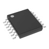
Available in 14-TSSOP Package

Product Advantages

Precise, low-noise, and low-power performance

Wide supply voltage and operating temperature ranges

Compact 14-TSSOP package

Key Technical Parameters

Number of Circuits: 4

Gain Bandwidth Product: 10MHz

Voltage Supply Span: 4.5V to 36V

Supply Current: 1.8mA per Amplifier

Slew Rate: 20V/µs

Input Offset Voltage: 1mV

Input Bias Current: 2pA

Output Current: 36mA per Amplifier

Quality and Safety Features

RoHS3 Compliant

Tape and Reel Packaging

Compatibility

Surface Mount, 14-TSSOP Package

Application Areas

Precision Measurement and Instrumentation

Data Acquisition Systems

Sensor Conditioning Circuits

High-Impedance Buffer Amplifiers

Low-Power Portable Equipment

Product Lifecycle

Currently available, no plans for discontinuation.

Replacement or upgrade options available if needed.

Key Reasons to Choose This Product

Excellent precision and low-noise performance

Wide operating voltage and temperature ranges

Compact and efficient 14-TSSOP package

RoHS3 compliance for environmental responsibility

Suitability for a wide range of precision analog applications

Frequently Asked Questions(FAQ)

What are the key performance differences between the OPA4141AIPWR and other J-FET amplifier ICs in terms of input bias current and voltage offset, and how do these parameters affect precision analog designs?
The OPA4141AIPWR exhibits an exceptionally low input bias current of just 2 pA, which is significantly lower than many competing J-FET amplifiers that typically range from 5 pA to over 100 pA. This ultra-low leakage current minimizes errors in high-impedance sensor interfaces and long-time-constant filtering applications, reducing drift and noise susceptibility. Additionally, its input voltage offset of 1 mV represents a moderate level for J-FET devices—lower than bipolar op-amps but higher than some zero-drift alternatives. While this offset may require trimming in ultra-high-precision systems, it remains acceptable for most industrial and instrumentation applications where cost and complexity trade-offs favor stability and bandwidth over absolute dc accuracy. Designers should consider whether the 1 mV offset introduces unacceptable gain error in their signal chain, especially when amplifying small differential signals through high-gain stages.
How does the supply voltage range and quiescent current of the OPA4141AIPWR compare to rail-to-rail operational amplifiers based on different internal architectures, and what design implications arise from these characteristics?
The OPA4141AIPWR operates across a wide supply span from 4.5 V to 36 V while consuming only 1.8 mA per four-channel package, resulting in approximately 450 µA per amplifier. This places it between CMOS-based rail-to-rail op-amps (which often consume less than 100 µA) and traditional bipolar designs. Compared to CMOS counterparts like the LMV324, the OPA4141 trades off power efficiency for superior speed and output drive capability. However, compared to other J-FET inputs such as the TL074, it offers much better rail-to-rail output swing and lower distortion at higher gains. For battery-powered or space-constrained designs requiring moderate bandwidth and high output current (up to 36 mA per channel), the OPA4141AIPWR provides a balanced compromise. Its ability to run on single supplies as low as 4.5 V makes it suitable for portable instrumentation, but engineers must account for the higher static current in long-running battery applications unless duty cycling is employed.
In what scenarios would the slew rate and gain bandwidth product of the OPA4141AIPWR become limiting factors, and how should they be evaluated against real-world analog signal requirements?
With a slew rate of 20 V/µs and a gain bandwidth product of 10 MHz, the OPA4141AIPWR is well-suited for general-purpose amplification but may struggle with fast transient signals above approximately 800 kHz at unity gain or large-amplitude pulses exceeding 500 V/µs peak-to-peak. For instance, driving a capacitive load beyond 1 nF into a high-gain stage could result in phase margin degradation due to limited open-loop response. In audio or precision data acquisition systems, this translates to acceptable performance, but in switched-capacitor circuits or ultrasonic sensing, faster amplifiers may be preferable. Engineers should calculate the required full-power bandwidth using the formula f = SR / (2πVp), ensuring that even at maximum output swing, the amplifier remains within its linear region without excessive ringing or overshoot.
What are the thermal and electrical limitations when driving capacitive loads with the OPA4141AIPWR, and how can stability be maintained in feedback-intensive configurations?
Driving capacitive loads directly can destabilize the OPA4141AIPWR due to its internal compensation and limited phase margin, particularly at gains greater than 10. While the device includes some internal protection, typical stability requires series isolation resistors (e.g., 5–20 Ω) between the output and capacitor, especially for loads exceeding 100 pF. At higher frequencies, the combination of output current limit (36 mA per channel) and capacitive reactance can cause current starvation, leading to droop or oscillation. In multi-stage filters or integrator applications, adding small lead-lag networks or using feedback capacitors in parallel with resistive feedback paths can improve phase margin. Thermal derating is minimal under normal conditions, but sustained output swings into heavy loads may elevate junction temperature, necessitating layout considerations near other heat sources in dense PCBs.
How does the moisture sensitivity level (MSL) rating of MSL 2 for the OPA4141AIPWR influence handling procedures during assembly, and what precautions should be taken before soldering in mass production environments?
The MSL 2 classification indicates that the OPA4141AIPWR can withstand one year of ambient storage before requiring bake-out if exposed to ambient conditions exceeding 30°C and 60% relative humidity for more than 168 hours. This means that after unpacking from tape-and-reel (TR) packaging, the components must either be used within seven days or stored in dry cabinets with desiccant monitoring. Failure to follow JEDEC J-STD-033 guidelines may lead to popcorning during reflow, compromising seal integrity and increasing risk of catastrophic failure. Production facilities should implement humidity monitoring logs and use conformal coating processes compatible with subsequent reliability testing. These measures ensure consistent solder joint quality and prevent latent defects related to moisture ingress in high-reliability applications such as automotive or medical systems.
Can the OPA4141AIPWR be safely substituted into existing designs using legacy J-FET amplifiers like the OP747ARUZ, and what compatibility issues might arise despite similar functionality?
Although the OP747ARUZ shares core features with the OPA4141AIPWR—such as J-FET input and rail-to-rail output—key differences exist that affect interchangeability. Most notably, the OP747 has a lower slew rate (~13 V/µs vs. 20 V/µs) and narrower supply range (typically ±15 V max vs. 36 V single-supply capability), making the OPA4141AIPWR unsuitable as a direct replacement in low-voltage or high-speed applications designed around the older part. Additionally, pinout and package dimensions differ slightly, requiring PCB modification. The OPA4141 also integrates four independent channels in a compact 14-pin TSSOP, whereas the OP747 often comes in larger packages with fewer channels. Therefore, while functionally similar, substitution demands careful evaluation of dynamic performance, power budget, and mechanical footprint before implementation.
What role does the input offset voltage of 1 mV play in closed-loop gain configurations using the OPA4141AIPWR, and how can system-level error budgets be affected by this parameter?
A 1 mV input offset voltage introduces a fixed error at the input that scales linearly with closed-loop gain. For example, in a non-inverting amplifier with a gain of 100, this results in an output error of 100 mV, which may saturate downstream ADCs or violate threshold tolerances in control loops. While external trimming could mitigate this, most applications accept the error if the total system error budget allows. However, in precision measurement chains involving multiple gain stages, accumulated offset errors can dominate over time. Designers should evaluate whether calibration routines or chopper-stabilized alternatives (like zero-drift amplifiers) are justified based on application tolerance requirements. In many industrial sensor conditioning circuits, however, the combination of low bias current and stable offset over temperature makes the OPA4141AIPWR a pragmatic choice despite its modest offset specification.
How does the operating temperature range of -40°C to 125°C impact long-term reliability and performance drift in harsh environment deployments using the OPA4141AIPWR?
The extended industrial-grade temperature range supports operation in automotive, aerospace, and downhole sensing applications where ambient extremes are common. Within this span, the OPA4141 maintains consistent gain, bandwidth, and offset behavior, though input offset voltage may vary up to ±2 mV over temperature depending on process variation. Long-term drift is influenced more by package stress and solder joint fatigue than intrinsic semiconductor aging, assuming proper thermal management. Thermal cycling tests indicate minimal parametric shift after thousands of cycles, provided PCB materials match CTE profiles to avoid mechanical strain. Still, users must validate end-system performance under actual field conditions rather than relying solely on datasheet extremes, since secondary effects like leakage through parasitic paths can emerge at temperature boundaries.
What considerations apply when cascading multiple gain stages using the OPA4141AIPWR in high-frequency signal chains, and how does the 10 MHz gain bandwidth product constrain overall system dynamics?
When designing multi-stage amplifiers, the cumulative effect of each stage’s finite gain-bandwidth product limits the achievable closed-loop bandwidth. Since the OPA4141AIPWR provides only 10 MHz GBW, a three-stage cascade with gains of 10, 10, and 10 will experience significant roll-off due to interaction between poles. Even conservative designs should maintain individual stage gains below 3 to preserve adequate phase margin. Additionally, interstage loading—especially capacitive coupling—can further reduce effective bandwidth. To maximize usable bandwidth, distributed amplification or active-RC techniques may be preferable. For broadband applications exceeding 2 MHz, alternative topologies like transimpedance amplifiers or specialized IF blocks might outperform simple cascaded op-amp stages using the OPA4141AIPWR.
How does the output drive capability of 36 mA per channel influence PCB layout decisions when using the OPA4141AIPWR in driving relays, LEDs, or other loads beyond standard resistive networks?
The 36 mA continuous output current enables direct switching of moderate loads such as optocouplers, small solenoids, or LED arrays without external buffers. However, this mandates careful attention to trace width, via placement, and thermal vias beneath the TSSOP pad to dissipate heat generated during prolonged conduction. Inductive loads require flyback diodes to protect against inductive kickback, which the device lacks internal protection against. Exceeding instantaneous current limits during startup or fault conditions risks latch-up or bond-wire failure, especially at elevated temperatures. Layout practices include minimizing loop inductance in power delivery paths and placing decoupling capacitors within 5 mm of the supply pins to stabilize dynamic current draw. These measures ensure robust operation and extend mean time between failures in mission-critical systems.
Why might the OPA4141AIPWR be preferred over CMOS-based rail-to-rail op-amps in certain high-impedance sensing applications, despite generally higher power consumption?
CMOS input stages typically exhibit flicker noise and higher 1/f corner frequencies, which degrade SNR in slow-changing, high-resistance sources such as piezoelectric sensors or thermopiles. The OPA4141AIPWR’s J-FET input offers extremely low DC bias current (2 pA) and reduced low-frequency noise, preserving signal fidelity over long integration times. Although it consumes more power (1.8 mA vs. ~500 µA for CMOS equivalents), the trade-off improves dynamic range and simplifies anti-aliasing filter design by avoiding noise peaking. Furthermore, J-FET inputs provide predictable transconductance and linear input capacitance, facilitating compensation network tuning. For applications where power budget permits and accuracy dominates efficiency concerns, the OPA4141AIPWR delivers superior performance in extracting weak signals buried in thermal noise.
What are the implications of the RoHS3 compliance and EAR99 classification for international sourcing and export control when selecting the OPA4141AIPWR for global product deployment?
RoHS3 compliance ensures the absence of restricted substances such as lead, mercury, and cadmium beyond specified thresholds, facilitating entry into EU markets and aligning with global sustainability regulations. The EAR99 designation indicates the OPA4141AIPWR is not subject to stringent export controls under U.S. regulations, simplifying procurement from distributors worldwide without ITAR restrictions. This lowers administrative overhead and accelerates time-to-market for commercial electronics manufacturers. Combined with REACH unaffected status, the component avoids supply chain delays associated with regulatory scrutiny. As a result, engineers can confidently specify the OPA4141AIPWR in consumer, industrial, and telecommunications equipment destined for North America, Europe, and Asia without anticipating licensing barriers or customs holdups.

Parts with Similar Specifications

The three parts on the right have similar specifications to Texas Instruments OPA4141AIPWR

Product Attribute OPA4140AIPWR OPA4141AIPW OPA4170AIPWR OPA4141AIDR
Part Number OPA4140AIPWR OPA4141AIPW OPA4170AIPWR OPA4141AIDR
Manufacturer Texas Instruments Texas Instruments Texas Instruments Texas Instruments
Slew Rate - - - -
Series - - - -
Mounting Type - Surface Mount Through Hole Surface Mount
Current - Supply - - - -
Base Product Number - DAC34H84 MAX500 ADS62P42
Current - Input Bias - - - -
Gain Bandwidth Product - - - -
Supplier Device Package - 196-NFBGA (12x12) 16-PDIP 64-VQFN (9x9)
Output Type - Current - Unbuffered Voltage - Buffered -
Voltage - Supply Span (Min) - - - -
Amplifier Type - - - -
Current - Output / Channel - - - -
Voltage - Supply Span (Max) - - - -
Operating Temperature - -40°C ~ 85°C 0°C ~ 70°C -40°C ~ 85°C
Voltage - Input Offset - - - -
Number of Circuits - - - -
Package - Tape & Reel (TR) Tube Tape & Reel (TR)
Package / Case - 196-LFBGA 16-DIP (0.300', 7.62mm) 64-VFQFN Exposed Pad

OPA4141AIPWR Datasheet PDF

Download OPA4141AIPWR pdf datasheets and Texas Instruments documentation for OPA4141AIPWR - Texas Instruments.

PCN Part Number
Device Symbolization Change 13/Jun/2023.pdf

Customer Reviews

Evaluation: 10 Articles

  • Nath***rooks
    Jun 11, 2026

    Installed this power component in a converter board. Output remained stable under different load conditions and thermal performance was better than expected.

  • Dani***alkerTech
    Jun 1, 2026

    Product works, but setup took more effort than expected. Once configured the MCU ran reliably, although documentation support felt older compared with newer platforms. Fine for maintenance projects.

  • Yuki***aka88
    May 26, 2026

    信号通信プロジェクトでこのRS-485トランシーバーを使用しました。設置は簡単で、長距離ケーブルでも通信は安定していました。消費電力も、以前使用していたものより低くなっています。

  • Stev***aker
    May 20, 2026

    Solid diode for power rectification. Works well in switching circuits.

  • Bran***Lewis
    May 11, 2026

    Compact FPGA with good performance. Suitable for basic signal processing tasks.

  • Oliv***arris
    May 7, 2026

    Reliable I/O expander. Works well in embedded control applications.

  • Jess***Jones
    Apr 17, 2026

    It offers good value for the price, and the specifications match the description. I’ve been using it for two days with no issues, and I’ll definitely buy it again if I need it in the future.

  • Mich***Smith
    Apr 17, 2026

    Shipping was on time, the component pins are neatly aligned, and I tested 10 of them with a multimeter—all readings were within the specified range. Highly recommended.

  • Aman***arris
    Apr 3, 2026

    It was great—the entire process, from placing the order to receiving the package, went very smoothly. The components were consistent, the price was fair, and I had a very pleasant shopping experience.

  • Mike***nch
    Apr 3, 2026

    Better than expected! The resistance and capacitance readings were spot-on, and it passed the test on the first try. The service was reliable, and the packaging was thoughtful—I highly recommend it.

Write a Review

Your Email address will not be published.

Shipment

Delivery Time

In-stock items can be shipped within 24 hours. Some parts will be arranged for delivery within 1-2 days from the date all items arrive at our warehouse. And Allelco ships order once a day at about 17:00, except Sunday. Once the goods are shipped, the estimated delivery time depends on the shipping methods and Delivery destination. The table below shows are the logistic time for some common countries.

Delivery Cost

  1. Use your express account for shipment if you have one.
  2. Use our account for the shipment. Refer to the table below for the approximate charges.
(Different time frame / countries / package size has different price.)

Delivery Method

  1. Global Common Shipment by DHL / UPS / FedEx / TNT / EMS / SF we support.
  2. Others more shipping ways, please get in touch with your customer manager.

Common Countries Logistic Time Reference
Region Country Logistic Time(Day)
America United States 5
Brazil 7
Europe Germany 5
United Kingdom 4
Italy 5
Oceania Australia 6
New Zealand 5
Asia India 4
Japan 4
Middle East Israel 6
DHL & FedEx Shipment Charges Reference
Shipment charges(KG) Reference DHL(USD$)
0.00kg-1.00kg USD$30.00 - USD$60.00
1.00kg-2.00kg USD$40.00 - USD$80.00
2.00kg-3.00kg USD$50.00 - USD$100.00
Note:
The above table is for reference only. There may have some data bias for the uncontrollable factors.
Contact us if you have any questions.
  • QC (Quality Warranty)
  • Payment Support
  • Packaging
  • Certifications & Memberships

QC (Quality Warranty)

Allelco is committed to exceeding customer expectations through customer service excellence, order accuracy, and on-time delivery.
This is achieved through our commitment to the continual improvement of our processes, services, and products.


Strict quality inspection builds a solid foundation for electronic component quality.
  1. Visual inspection
  2. Performance testing and reliability verification
  3. Standardized full-process testing
  4. Precise control of every parameter
We eliminate defective components and ensure the stable operation of electronic devices through professional quality standards.

Payment Support

The payment method can be chosen from the methods shown below: Wire Transfer (T/T, Bank Transfer), Western Union, Credit card, PayPal.
  • HKBea
  • Paypal
  • MasterCard
  • Western-Union
  • VISA
Stable Delivery, Sincere Partnership — Your Faithful Supply Chain Partner
  • Efficient Supply Management
  • Cost-Saving Procurement
  • Fast Sourcing & Delivery
Contact us if you have any questions.

Packaging

Electrostatic Discharge Protection and Handling

All electrostatic-sensitive components are handled in accordance with electrostatic discharge control procedures. The products are hermetically sealed in anti-static safe packaging to prevent electrostatic damage. Appropriate labeling is also applied for identification and traceability. This ensures product integrity during storage, handling and transportation.


ESD

Certifications & Memberships

Third-party certified, strict quality control. Our certification
  • ISO 9001: 2015
  • ISO 13485: 2016
  • ISO 14001: 2015
  • ISO 28000: 2007
  • ISO 45001: 2018
  • GB/T 27922-2011
  • SMTA
  • IPC
  • ESD
  • PSMA
OPA4141AIPWR Image

OPA4141AIPWR

Texas Instruments
32D-OPA4141AIPWR

Want a better price? Add to Cart and Submit RFQ now, we'll contact you immediately.

0 RFQ
Shopping cart (0 Items)
It is empty.
Compare List (0 Items)
It is empty.
Feedback

Your feedback matters! At Allelco, we value the user experience and strive to improve it constantly.
Please share your comments with us via our feedback form, and we'll respond promptly.
Thank you for choosing Allelco.

Subject
E-mail
Comments
Captcha
Drag or click to upload file
Upload File
types: .xls, .xlsx, .doc, .docx, .jpg, .png and .pdf.
Max file size: 10MB