
OPA4354AIPWT (1)
Manufacturer Part Number
OPA4354AIPWT
Manufacturer
Texas Instruments
Introduction
High-performance, low-noise, quad operational amplifier
Ideal for instrumentation, control, and precision analog applications
Product Features and Performance
Quad op-amp in a single package
Wide supply voltage range: 2.5V to 5.5V
Rail-to-rail input and output
Low input offset voltage: 2mV
High gain bandwidth product: 100MHz
High slew rate: 150V/μs
Low input bias current: 3pA
-3dB bandwidth: 250MHz
Low noise: 8nV/√Hz
Operates from -40°C to 125°C
Product Advantages
Excellent DC and AC performance
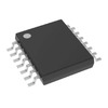
Compact 14-TSSOP package
Ease of design and implementation
Key Technical Parameters
Number of Circuits: 4
Gain Bandwidth Product: 100MHz
Supply Voltage Range: 2.5V to 5.5V
Supply Current: 4.9mA per channel
Slew Rate: 150V/μs
Input Offset Voltage: 2mV
Input Bias Current: 3pA
-3dB Bandwidth: 250MHz
Quality and Safety Features
RoHS3 compliant
Suitable for industrial and commercial applications
Compatibility
Surface mount 14-TSSOP package
Compatible with a wide range of electronic systems and designs
Application Areas
Instrumentation and control systems
Precision analog circuits
Data acquisition and processing
Sensor conditioning
Audio and video signal processing
Product Lifecycle
Currently available
No known plans for discontinuation
Replacements and upgrades may be available in the future
Several Key Reasons to Choose This Product
Excellent DC and AC performance for high-precision applications
Compact 14-TSSOP package for space-constrained designs
Wide operating temperature range (-40°C to 125°C)
Low power consumption and heat dissipation
RoHS3 compliance for environmental and safety considerations
Ease of design and implementation with quad op-amp in a single package


 OPA4364AIDRG4Texas InstrumentsIC CMOS 4 CIRCUIT 14SOIC
 OPA4354AIDRTexas InstrumentsIC CMOS 4 CIRCUIT 14SOIC
 OPA4354AQPWRQ1Texas InstrumentsIC CMOS 4 CIRCUIT 14TSSOP
 OPA4354ABURR-BROWN


