View All

Please refer to the English Version as our Official Version.Return

Europe
France(Français) Germany(Deutsch) Italy(Italia) Russian(русский) Poland(polski) Czech(Čeština) Luxembourg(Lëtzebuergesch) Netherlands(Nederland) Iceland(íslenska) Hungarian(Magyarország) Spain(español) Portugal(Português) Turkey(Türk dili) Bulgaria(Български език) Ukraine(Україна) Greece(Ελλάδα) Israel(עִבְרִית) Sweden(Svenska) Finland(Svenska) Finland(Suomi) Romania(românesc) Moldova(românesc) Slovakia(Slovenská) Denmark(Dansk) Slovenia(Slovenija) Slovenia(Hrvatska) Croatia(Hrvatska) Serbia(Hrvatska) Montenegro(Hrvatska) Bosnia and Herzegovina(Hrvatska) Lithuania(lietuvių) Spain(Português) Switzerland(Deutsch) United Kingdom(English)
Asia/Pacific
Japan(日本語) Korea(한국의) Thailand(ภาษาไทย) Malaysia(Melayu) Singapore(Melayu) Vietnam(Tiếng Việt) Philippines(Pilipino)
Africa, India and Middle East
United Arab Emirates(العربية) Iran(فارسی) Tajikistan(فارسی) India(हिंदी) Madagascar(malaɡasʲ)
South America / Oceania
New Zealand(Maori) Brazil(Português) Angola(Português) Mozambique(Português)
North America
United States(English) Canada(English) Haiti(Ayiti) Mexico(español)
HomeProductsIntegrated Circuits (ICs)Linear - Amplifiers - Instrumentation, OP Amps, Buffer AmpsOPA653IDRBR
OPA653IDRBR Image
Image may be representation.
See specifications for product details.
EXPRESS OPTION
Payment method

OPA653IDRBR - Texas Instruments

Manufacturer Part Number
OPA653IDRBR
Manufacturer
Texas Instruments
Allelco Part Number
32D-OPA653IDRBR
Warranty
1 Year Allelco Warranty - Find out more
Stock Status:
14,170 pcs available, New & Original
Parts Description
IC OPAMP JFET 1 CIRCUIT 8SON
Package
8-SON (3x3)
Data sheet
-
RoHs Status
ROHS3 Compliant
Our certification
In stock: 14170

Required fields are indicated by an asterisk (*)
Please send RFQ, we will respond immediately.

Quantity

Specifications

OPA653IDRBR Tech Specifications
Texas Instruments - OPA653IDRBR technical specifications, attributes, parameters and parts with similar specifications to Texas Instruments - OPA653IDRBR

Product Attribute Attribute Value
Manufacturer Texas Instruments
Voltage - Supply Span (Min) 7 V
Voltage - Supply Span (Max) 13 V
Voltage - Input Offset 1 mV
Supplier Device Package 8-SON (3x3)
Slew Rate 2675V/µs
Series -
Package / Case 8-VDFN Exposed Pad
Package Tape & Reel (TR)
Output Type -
Product Attribute Attribute Value
Operating Temperature -40°C ~ 85°C
Number of Circuits 1
Mounting Type Surface Mount
Current - Supply 32mA
Current - Output / Channel 70 mA
Current - Input Bias 10 pA
Base Product Number OPA653
Amplifier Type J-FET
-3db Bandwidth 500 MHz

Environmental & Export Classifications

ATTRIBUTE DESCRIPTION
RoHs Status ROHS3 Compliant
Moisture Sensitivity Level (MSL) 2 (1 Year)
REACH Status REACH Unaffected
ECCN EAR99

Parts Introduction

OPA653IDRBR Image
OPA653IDRBR (1)

Manufacturer Part Number

OPA653IDRBR

Manufacturer

Texas Instruments

Introduction

High-Speed, Low-Noise, Rail-to-Rail, JFET Input Operational Amplifier

Product Features and Performance

Wide Bandwidth of 500 MHz

High Slew Rate of 2675 V/μs

Low Input Offset Voltage of 1 mV

Low Input Bias Current of 10 pA

Wide Supply Voltage Range from 7 V to 13 V

Low Supply Current of 32 mA

High Output Current of 70 mA

Wide Operating Temperature Range from -40°C to 85°C

Product Advantages

Excellent AC performance for wide range of applications

Suitable for high-speed, low-noise instrumentation

Capable of driving capacitive loads

Key Technical Parameters

Voltage Supply Span (Min): 7 V

Voltage Supply Span (Max): 13 V

Current Supply: 32 mA

Slew Rate: 2675 V/s

Voltage Input Offset: 1 mV

Amplifier Type: J-FET

Current Output / Channel: 70 mA

Current Input Bias: 10 pA

-3dB Bandwidth: 500 MHz

Quality and Safety Features

RoHS3 Compliant

Compatibility

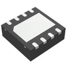
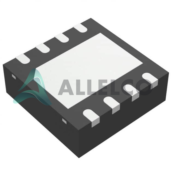
8-VDFN Exposed Pad package

Surface Mount Mounting Type

Application Areas

High-speed instrumentation

Video amplifiers

Precision analog circuits

Driving capacitive loads

Product Lifecycle

Current product, no discontinuation planned

Replacements or upgrades may be available

Several Key Reasons to Choose This Product

Excellent high-speed, low-noise performance

Wide supply voltage and temperature ranges

Capable of driving capacitive loads

Compact and efficient 8-VDFN package

RoHS3 compliance for environmental safety
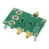
Frequently Asked Questions(FAQ)

How does the OPA653IDRBR’s slew rate and bandwidth compare to typical bipolar input op-amps when driving high-speed analog signals in RF front-end applications?
The OPA653IDRBR delivers a 2675 V/µs slew rate and 500 MHz gain-bandwidth product, significantly exceeding most bipolar op-amps that typically offer slew rates below 100 V/µs and bandwidth under 100 MHz. This enables precise handling of fast transient responses and wideband amplification without excessive phase distortion. In RF front-end designs requiring large-signal fidelity across multiple octaves, this performance reduces settling time and improves dynamic range compared to lower-speed alternatives.
What design considerations arise when using the OPA653IDRBR in single-supply configurations near its minimum supply voltage of 7 V, especially regarding output swing and headroom?
Operating near the 7 V minimum supply demands careful attention to output stage headroom. With a typical rail-to-rail capability limited by internal architecture, the maximum output swing may be only 1.5–2 V from each supply rail under moderate load conditions. At 7 V total supply, this leaves approximately ±2.5 V available for signal excursion, which may restrict use in precision DC-coupled stages unless input common-mode and output swing requirements are tightly managed. Proper biasing and signal scaling become critical to avoid clipping or nonlinear behavior.
How does the input bias current of the OPA653IDRBR—10 pA typical—affect high-impedance sensor interface circuits such as piezoelectric accelerometers or photodetector readout stages?
At 10 pA bias current, leakage paths through source resistors or PCB contamination can introduce significant offset errors in high-impedance nodes. For example, a 1 GΩ feedback resistor would produce a 10 mV offset due solely to bias current—comparable to the device’s 1 mV input offset voltage. This necessitates guarding techniques, low-leakage layout practices, and possibly periodic calibration in long-term monitoring systems where drift matters more than initial accuracy.
In what scenarios would substituting the OPA653IDRBR with the OPA653IDBVT be justified despite differences in package footprint, and how do pin functions compare between these two models?
The OPA653IDBVT uses a smaller SOT-23-8 package instead of the DFN, making it suitable for space-constrained portable instrumentation where board real estate is premium. However, thermal performance degrades due to reduced exposed pad connectivity. Pin compatibility allows direct replacement in non-heat-critical applications, but designers must verify solder joint reliability under vibration or thermal cycling. The core electrical specifications remain identical, so signal integrity is preserved if layout parasitics are controlled.
What are the implications of the OPA653IDRBR’s 32 mA supply current on power budgeting in battery-powered wireless sensor nodes operating at 10 MHz switching frequency?
Drawing 32 mA at full swing implies a power dissipation of roughly 0.22 W at 7 V (32 mA × 7 V), which is substantial for energy harvesting systems. Even with duty-cycling, average current may exceed 5 mA depending on signal activity. This forces trade-offs between speed and longevity—alternatives like lower-power JFET op-amps may extend runtime but sacrifice bandwidth and slew rate. Thermal management becomes essential if continuous operation occurs within confined enclosures.
How should PCB layout be approached when routing high-speed differential signals adjacent to the OPA653IDRBR’s power pins to minimize noise coupling and ensure stability?
Due to its 500 MHz bandwidth, the OPA653IDRBR is sensitive to power supply impedance above 10 MHz. Place decoupling capacitors—preferably 100 nF X7R ceramic—directly at the V+ and V− pins with minimal trace length. Maintain guard rings around input traces and avoid routing sensitive feedback loops over split planes. Ground plane continuity under the 8-SON (3x3) package enhances thermal dissipation and reduces ground bounce, which can destabilize high-gain configurations.
Can the OPA653IDRBR drive capacitive loads beyond 100 pF without additional isolation circuitry, and what risks exist if used in unity-gain buffer mode?
While capable of driving moderate capacitive loads, driving >100 pF in unity-gain configuration risks oscillation due to internal compensation interacting with stray capacitance. A series isolation resistor (e.g., 2–10 Ω) at the output node is recommended to dampen peaking. Without it, peaking above 3 dB or ringing may occur during step transitions, corrupting signal integrity in ADC driver or video amplifier roles where waveform purity is paramount.
What environmental and compliance factors must be verified before deploying the OPA653IDRBR in industrial automation equipment certified for EU markets?
Although RoHS3 compliant and REACH unaffected, designers must confirm end-product conformity with EMC directives (EN 61000-6-4) and functional safety standards (IEC 61508) if used in safety-related control loops. The MSL 2 classification allows one year shelf life after opening, but humidity-induced failures can still occur if storage exceeds recommended conditions. Additionally, export controls under ECCN EAR99 permit global distribution, but local import regulations may apply based on final assembly country.

Parts with Similar Specifications

The three parts on the right have similar specifications to Texas Instruments OPA653IDRBR

Product Attribute OPA653IDBVR OPA656MDREP OPA651UB OPA656N/250G4
Part Number OPA653IDBVR OPA656MDREP OPA651UB OPA656N/250G4
Manufacturer Texas Instruments Texas Instruments Texas Instruments Texas Instruments
Slew Rate - - - -
Series - - - -
Current - Supply - - - -
Number of Circuits - - - -
-3db Bandwidth - - - -
Package - Tape & Reel (TR) Tube Tape & Reel (TR)
Voltage - Supply Span (Min) - - - -
Output Type - Current - Unbuffered Voltage - Buffered -
Mounting Type - Surface Mount Through Hole Surface Mount
Current - Output / Channel - - - -
Voltage - Supply Span (Max) - - - -
Supplier Device Package - 196-NFBGA (12x12) 16-PDIP 64-VQFN (9x9)
Base Product Number - DAC34H84 MAX500 ADS62P42
Current - Input Bias - - - -
Operating Temperature - -40°C ~ 85°C 0°C ~ 70°C -40°C ~ 85°C
Voltage - Input Offset - - - -
Amplifier Type - - - -
Package / Case - 196-LFBGA 16-DIP (0.300', 7.62mm) 64-VFQFN Exposed Pad

Customer Reviews

Evaluation: 10 Articles

  • Nath***rooks
    Jun 11, 2026

    Installed this power component in a converter board. Output remained stable under different load conditions and thermal performance was better than expected.

  • Dani***alkerTech
    Jun 1, 2026

    Product works, but setup took more effort than expected. Once configured the MCU ran reliably, although documentation support felt older compared with newer platforms. Fine for maintenance projects.

  • Yuki***aka88
    May 26, 2026

    信号通信プロジェクトでこのRS-485トランシーバーを使用しました。設置は簡単で、長距離ケーブルでも通信は安定していました。消費電力も、以前使用していたものより低くなっています。

  • Stev***aker
    May 20, 2026

    Solid diode for power rectification. Works well in switching circuits.

  • Bran***Lewis
    May 11, 2026

    Compact FPGA with good performance. Suitable for basic signal processing tasks.

  • Oliv***arris
    May 7, 2026

    Reliable I/O expander. Works well in embedded control applications.

  • Jess***Jones
    Apr 17, 2026

    It offers good value for the price, and the specifications match the description. I’ve been using it for two days with no issues, and I’ll definitely buy it again if I need it in the future.

  • Mich***Smith
    Apr 17, 2026

    Shipping was on time, the component pins are neatly aligned, and I tested 10 of them with a multimeter—all readings were within the specified range. Highly recommended.

  • Aman***arris
    Apr 3, 2026

    It was great—the entire process, from placing the order to receiving the package, went very smoothly. The components were consistent, the price was fair, and I had a very pleasant shopping experience.

  • Mike***nch
    Apr 3, 2026

    Better than expected! The resistance and capacitance readings were spot-on, and it passed the test on the first try. The service was reliable, and the packaging was thoughtful—I highly recommend it.

Write a Review

Your Email address will not be published.

Shipment

Delivery Time

In-stock items can be shipped within 24 hours. Some parts will be arranged for delivery within 1-2 days from the date all items arrive at our warehouse. And Allelco ships order once a day at about 17:00, except Sunday. Once the goods are shipped, the estimated delivery time depends on the shipping methods and Delivery destination. The table below shows are the logistic time for some common countries.

Delivery Cost

  1. Use your express account for shipment if you have one.
  2. Use our account for the shipment. Refer to the table below for the approximate charges.
(Different time frame / countries / package size has different price.)

Delivery Method

  1. Global Common Shipment by DHL / UPS / FedEx / TNT / EMS / SF we support.
  2. Others more shipping ways, please get in touch with your customer manager.

Common Countries Logistic Time Reference
Region Country Logistic Time(Day)
America United States 5
Brazil 7
Europe Germany 5
United Kingdom 4
Italy 5
Oceania Australia 6
New Zealand 5
Asia India 4
Japan 4
Middle East Israel 6
DHL & FedEx Shipment Charges Reference
Shipment charges(KG) Reference DHL(USD$)
0.00kg-1.00kg USD$30.00 - USD$60.00
1.00kg-2.00kg USD$40.00 - USD$80.00
2.00kg-3.00kg USD$50.00 - USD$100.00
Note:
The above table is for reference only. There may have some data bias for the uncontrollable factors.
Contact us if you have any questions.
  • QC (Quality Warranty)
  • Payment Support
  • Packaging
  • Certifications & Memberships

QC (Quality Warranty)

Allelco is committed to exceeding customer expectations through customer service excellence, order accuracy, and on-time delivery.
This is achieved through our commitment to the continual improvement of our processes, services, and products.


Strict quality inspection builds a solid foundation for electronic component quality.
  1. Visual inspection
  2. Performance testing and reliability verification
  3. Standardized full-process testing
  4. Precise control of every parameter
We eliminate defective components and ensure the stable operation of electronic devices through professional quality standards.

Payment Support

The payment method can be chosen from the methods shown below: Wire Transfer (T/T, Bank Transfer), Western Union, Credit card, PayPal.
  • HKBea
  • Paypal
  • MasterCard
  • Western-Union
  • VISA
Stable Delivery, Sincere Partnership — Your Faithful Supply Chain Partner
  • Efficient Supply Management
  • Cost-Saving Procurement
  • Fast Sourcing & Delivery
Contact us if you have any questions.

Packaging

Electrostatic Discharge Protection and Handling

All electrostatic-sensitive components are handled in accordance with electrostatic discharge control procedures. The products are hermetically sealed in anti-static safe packaging to prevent electrostatic damage. Appropriate labeling is also applied for identification and traceability. This ensures product integrity during storage, handling and transportation.


ESD

Certifications & Memberships

Third-party certified, strict quality control. Our certification
  • ISO 9001: 2015
  • ISO 13485: 2016
  • ISO 14001: 2015
  • ISO 28000: 2007
  • ISO 45001: 2018
  • GB/T 27922-2011
  • SMTA
  • IPC
  • ESD
  • PSMA
OPA653IDRBR Image

OPA653IDRBR

Texas Instruments
32D-OPA653IDRBR

Want a better price? Add to Cart and Submit RFQ now, we'll contact you immediately.

0 RFQ
Shopping cart (0 Items)
It is empty.
Compare List (0 Items)
It is empty.
Feedback

Your feedback matters! At Allelco, we value the user experience and strive to improve it constantly.
Please share your comments with us via our feedback form, and we'll respond promptly.
Thank you for choosing Allelco.

Subject
E-mail
Comments
Captcha
Drag or click to upload file
Upload File
types: .xls, .xlsx, .doc, .docx, .jpg, .png and .pdf.
Max file size: 10MB