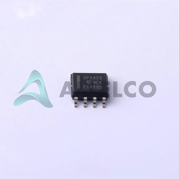
View All

Please refer to the English Version as our Official Version.Return

Europe
France(Français) Germany(Deutsch) Italy(Italia) Russian(русский) Poland(polski) Czech(Čeština) Luxembourg(Lëtzebuergesch) Netherlands(Nederland) Iceland(íslenska) Hungarian(Magyarország) Spain(español) Portugal(Português) Turkey(Türk dili) Bulgaria(Български език) Ukraine(Україна) Greece(Ελλάδα) Israel(עִבְרִית) Sweden(Svenska) Finland(Svenska) Finland(Suomi) Romania(românesc) Moldova(românesc) Slovakia(Slovenská) Denmark(Dansk) Slovenia(Slovenija) Slovenia(Hrvatska) Croatia(Hrvatska) Serbia(Hrvatska) Montenegro(Hrvatska) Bosnia and Herzegovina(Hrvatska) Lithuania(lietuvių) Spain(Português) Switzerland(Deutsch) United Kingdom(English)
Asia/Pacific
Japan(日本語) Korea(한국의) Thailand(ภาษาไทย) Malaysia(Melayu) Singapore(Melayu) Vietnam(Tiếng Việt) Philippines(Pilipino)
Africa, India and Middle East
United Arab Emirates(العربية) Iran(فارسی) Tajikistan(فارسی) India(हिंदी) Madagascar(malaɡasʲ)
South America / Oceania
New Zealand(Maori) Brazil(Português) Angola(Português) Mozambique(Português)
North America
United States(English) Canada(English) Haiti(Ayiti) Mexico(español)
HomeProductsIntegrated Circuits (ICs)Linear - Amplifiers - Instrumentation, OP Amps, Buffer AmpsOPA828IDR
OPA828IDR Image
Image may be representation.
See specifications for product details.
EXPRESS OPTION
Payment method

OPA828IDR - Texas Instruments

Manufacturer Part Number
OPA828IDR
Manufacturer
Texas Instruments
Allelco Part Number
32D-OPA828IDR
Warranty
1 Year Allelco Warranty - Find out more
Stock Status:
10,357 pcs available, New & Original
Parts Description
IC OPAMP JFET 1 CIRCUIT 8SOIC
Package
8-SOIC
Data sheet
OPA828IDR.pdf
RoHs Status
ROHS3 Compliant
Our certification
In stock: 10357
  • Unit Price: $2.605
  • Subtotal: $0.00

Want a better price?
Add to Cart and Submit RFQ now, we'll contact you immediately.

Quantity Unit Price Ext. Price
1+ $2.605 $2.61
10+ $2.255 $22.55
30+ $2.048 $61.44
100+ $1.838 $183.80
500+ $1.741 $870.50
1000+ $1.697 $1,697.00
The above prices does not include taxes and freight rates, which will be calculated on the order pages.

Specifications

OPA828IDR Tech Specifications
Texas Instruments - OPA828IDR technical specifications, attributes, parameters and parts with similar specifications to Texas Instruments - OPA828IDR

Product Attribute Attribute Value
Manufacturer Texas Instruments
Voltage - Supply Span (Min) 8 V
Voltage - Supply Span (Max) 36 V
Voltage - Input Offset 50 µV
Supplier Device Package 8-SOIC
Slew Rate 150V/µs
Series -
Package / Case 8-SOIC (0.154", 3.90mm Width)
Package Tape & Reel (TR)
Output Type -
Product Attribute Attribute Value
Operating Temperature -40°C ~ 125°C
Number of Circuits 1
Mounting Type Surface Mount
Gain Bandwidth Product 45 MHz
Current - Supply 5.5mA
Current - Output / Channel 30 mA
Current - Input Bias 1 pA
Base Product Number OPA828
Amplifier Type J-FET

Environmental & Export Classifications

ATTRIBUTE DESCRIPTION
RoHs Status ROHS3 Compliant
Moisture Sensitivity Level (MSL) 2 (1 Year)
REACH Status REACH Unaffected
ECCN EAR99

Parts Introduction

OPA828IDR Image
OPA828IDR (1)

Manufacturer Part Number

OPA828IDR

Manufacturer

Texas Instruments

Introduction

High-precision, high-speed operational amplifier

Designed for instrumentation and data acquisition applications

Product Features and Performance

Wide supply voltage range of 8V to 36V

Low input bias current of 1pA

High gain bandwidth of 45MHz

Slew rate of 150V/μs

Rail-to-rail input and output

Stable with capacitive loads

Product Advantages

Excellent DC precision and AC performance

Suitable for a wide range of applications

Reliable and robust design

OPA828IDR Image
OPA828IDR (2)

Key Technical Parameters

Operating temperature range: -40°C to 125°C

Supply current: 5.5mA

Output current: 30mA

Input offset voltage: 50μV

Quality and Safety Features

RoHS3 compliant

8-SOIC surface mount package

Compatibility

Compatible with a wide range of electronic systems and instrumentation

Application Areas

Instrumentation and data acquisition

Medical equipment

Industrial control systems

Test and measurement equipment

Product Lifecycle

Currently in production

Replacements and upgrades available

Several Key Reasons to Choose This Product

Exceptional DC and AC performance

Wide operating temperature range

Low power consumption

Compact and robust package

Proven reliability and long-term availability

Frequently Asked Questions(FAQ)

How does the OPA828IDR's input bias current of 1 pA compare to CMOS and bipolar op-amps in high-impedance sensor applications, and what design considerations does this necessitate?
The OPA828IDR exhibits an exceptionally low input bias current of 1 pA, which places it among the best-in-class JFET-input amplifiers. In contrast, typical CMOS op-amps often have input bias currents in the femtoampere (fA) range, while bipolar designs usually operate in the nanoampere (nA) range. Despite this distinction, the 1 pA level is still significant enough in high-impedance circuits—such as those involving piezoelectric sensors or high-value feedback networks—to require careful layout practices, including minimizing trace resistance and avoiding contamination from handling or PCB flux residues. Designers should also consider guard rings and proper grounding techniques to prevent leakage currents from dominating over the specified bias current.
What are the implications of the OPA828IDR’s 150 V/µs slew rate when driving capacitive loads in precision analog front ends, especially at full output swing?
With a slew rate of 150 V/µs, the OPA828IDR can handle moderate-speed transient signals common in audio and instrumentation systems, but it may struggle with fast edge rates when driving large capacitive loads near supply rails. For example, a 10 nF load with a 30 V step would theoretically require only ~2 µs to settle, which seems manageable; however, actual performance depends on how close the output swing is to the supply rails due to internal compensation limitations. In high-gain configurations or under large-signal conditions, the amplifier may exhibit overshoot or ringing if the capacitive load exceeds stability margins. Therefore, stability analysis using phase margin and recommended compensation techniques is essential for reliable operation.
Can the OPA828IDR be used in single-supply battery-powered applications requiring rail-to-rail input and output swing across a 4.5 V to 36 V supply range?
While the OPA828IDR supports a wide supply range from 8 V to 36 V, it is not specified as a rail-to-rail input/output (RRIO) device. Its input stage is based on JFET technology, which typically allows input voltages within approximately 1.5 V of the negative rail but does not guarantee full rail access. Similarly, the output swing will likely be limited to within a few volts of each rail unless operated above 12 V. For true RRIO performance in low-voltage single-supply designs—especially below 8 V—alternative devices such as CMOS-based RRIO op-amps would be more appropriate. Thus, the OPA828IDR is better suited for higher-voltage, dual-supply or well-biased single-supply applications where headroom is available.
How does the gain bandwidth product (GBW) of 45 MHz influence closed-loop bandwidth when using the OPA828IDR in non-inverting configurations with gains greater than unity?
The OPA828IDR offers a gain bandwidth product of 45 MHz, meaning that in a unity-gain buffer configuration, it can maintain bandwidth up to 45 MHz before gain begins to roll off. However, in higher-gain applications—for instance, a non-inverting amplifier set to a gain of +10—the effective bandwidth drops inversely with gain: approximately 4.5 MHz. This relationship holds under ideal conditions, but real-world limitations such as parasitic capacitance, PCB layout parasitics, and load impedance further reduce usable bandwidth. Designers must therefore select gain values that align with signal frequency requirements to avoid excessive phase lag and potential instability.
What thermal and power dissipation concerns arise when operating the OPA828IDR continuously at maximum ambient temperature (125°C), given its quiescent current of 5.5 mA per channel?
At a supply voltage of ±15 V (common in precision analog systems), the OPA828IDR consumes approximately 5.5 mA × 30 V = 165 mW per channel under no-load conditions. If operating continuously at 125°C ambient without airflow or heatsinking, the junction-to-ambient thermal resistance (θJA) must be considered. Assuming a typical θJA of 150°C/W for an 8-SOIC package mounted on a standard FR4 PCB, the estimated rise above ambient would be 165 mW × 150°C/W = 24.75°C, resulting in a junction temperature of about 150°C—approaching absolute maximum ratings. Therefore, continuous high-power operation near upper temperature limits may require derating, improved thermal management, or reduced supply voltage to ensure reliability.
When comparing the OPA828IDR to the OPA695 or OPA140, which one is preferable for low-noise, high-precision DC amplification in medical instrumentation?
Although all three devices offer excellent DC precision, the choice depends on specific noise and speed requirements. The OPA828IDR features a voltage offset of 50 µV and low bias current, making it suitable for moderate-speed DC applications. The OPA140, by contrast, provides even lower input voltage noise (typically <10 nV/√Hz) and higher open-loop gain, favoring ultra-high-impedance sources like pH probes or biosensors. Meanwhile, the OPA695 delivers superior speed (slew rate >500 V/µs) and GBW (>1 GHz), targeting RF and high-frequency precision tasks. For medical instrumentation emphasizing accuracy and stability over bandwidth, the OPA140 might edge out due to its enhanced noise performance and drift characteristics, whereas the OPA828IDR remains a strong candidate where moderate bandwidth and cost efficiency are acceptable.
Is the OPA828IDR suitable for use in automotive-grade environments requiring AEC-Q100 qualification, and what alternatives exist if certification is mandatory?
No, the OPA828IDR is not qualified to AEC-Q100 standards and is intended for commercial and industrial use. For automotive applications demanding functional safety and environmental resilience, TI offers the OPA847 or OPA2847, which are AEC-Q100 Grade 1 certified (-40°C to +125°C). These variants maintain similar electrical performance but undergo rigorous testing for long-term reliability in harsh conditions. If the application involves in-vehicle sensing, motor control, or infotainment systems, substituting the OPA828IDR with its automotive counterpart becomes necessary to meet OEM requirements and regulatory compliance.
How should decoupling capacitors be selected and placed to ensure stable operation of the OPA828IDR in space-constrained PCB layouts?
Stable operation of the OPA828IDR requires proper power supply decoupling due to its relatively high quiescent current (5.5 mA). A combination of a 10 µF bulk capacitor (e.g., ceramic X5R/X7R) located near the power entry point and a 0.1 µF ceramic capacitor placed within 1 cm of the V+ and V− pins minimizes high-frequency noise and prevents oscillation. Additionally, a 10 nF capacitor should be placed as close as possible to the IC to filter supply transients. Layout priority includes short, wide traces, avoiding vias near sensitive nodes, and separating analog and digital ground planes. Poor decoupling can manifest as increased noise floor, reduced PSRR, or even intermittent instability during dynamic load changes.
What are the risks of exceeding the 30 mA output current capability of the OPA828IDR, and how can overcurrent protection be implemented in the absence of internal foldback?
The OPA828IDR specifies a maximum output current of 30 mA per channel, beyond which internal thermal mechanisms may activate but without guaranteed protection. Exceeding this limit risks localized heating, increased distortion, or permanent damage to the output stage. Since there is no integrated current limiting, external current-sense resistors or MOSFET-based active current limiters can be added in series with the load. Alternatively, feedback control loops incorporating shunt monitoring can dynamically adjust gain or disable the driver if sustained overload occurs. Such measures are particularly important in fault-tolerant systems like test equipment or battery-powered actuators, where unexpected shorts could otherwise compromise both the amplifier and connected circuitry.
How does the input offset voltage drift of the OPA828IDR (±0.5 µV/°C typical) affect long-term calibration stability in precision data acquisition systems?
Over a temperature range of -40°C to +125°C (a span of 165°C), the OPA828IDR’s input offset voltage drift contributes approximately ±82.5 µV variation in worst-case scenarios. Given its initial offset of 50 µV, total offset error can reach ±132.5 µV. In high-gain, low-level signal paths—such as bridge transducers or thermocouple amplifiers—this drift may exceed allowable thresholds for system accuracy. To mitigate, designers often employ offset null pins (if available) or implement software calibration routines that periodically measure and compensate for drift. Alternatively, selecting amplifiers with lower drift coefficients or using chopper-stabilized architectures may yield superior long-term stability, depending on system budget and complexity constraints.
What layout precautions are critical when routing feedback networks around the OPA828IDR to minimize parasitic capacitance and leakage?
Due to the OPA828IDR’s high impedance inputs (JFET structure) and sensitivity to stray effects, feedback resistors should be placed close to the amplifier with minimal exposed copper between input pins and feedback traces. Use surface-mount chip resistors with tight tolerance and low TCR to avoid introducing additional mismatch errors. Avoid routing feedback lines parallel to noisy digital traces or high-current paths, and consider adding small guard traces grounded at a single point near the input to shield against capacitive coupling. Also, keep input traces short and shielded from humidity or ionic contamination, which could elevate effective input current and degrade CMRR.
Can the OPA828IDR drive heavy capacitive loads directly, and what compensation techniques improve stability in such configurations?
Directly driving large capacitive loads—such as cables or unterminated transmission lines—can destabilize the OPA828IDR due to insufficient phase margin. A common solution is to insert a small series isolation resistor (typically 22 Ω to 100 Ω) between the amplifier output and the capacitive load, forming an RC network that reduces peaking. This technique effectively increases damping and extends stability into higher-capacitance regimes. For very large loads (e.g., >100 pF), additional compensation such as a zeroing resistor in parallel with the feedback capacitor may be required. Always verify stability via simulation or bench testing, as the optimal approach depends on exact load value, gain setting, and signal integrity requirements.
How does the OPA828IDR perform in terms of common-mode rejection ratio (CMRR) and power supply rejection ratio (PSRR), and why do these matter in industrial environments?
While explicit CMRR and PSRR numbers are not listed in the key parameters, JFET-input amplifiers like the OPA828IDR generally exhibit high CMRR (>100 dB) and moderate-to-good PSRR (~70–90 dB at mid frequencies). In industrial settings with fluctuating supply voltages, switching regulators, or ground loops, degraded PSRR can introduce supply-induced noise into the output. Similarly, poor CMRR allows common-mode interference (e.g., EMI from motors or relays) to appear differentially. Ensuring clean, well-regulated supplies and symmetrical layout symmetry enhances both ratios. If stringent rejection is needed, post-amplification filtering or instrumentation-grade amplifiers with explicitly rated CMRR/PSRR should be evaluated instead.
What role does the moisture sensitivity level (MSL) of 2 play during assembly, and how should storage conditions affect procurement planning for the OPA828IDR?
With an MSL rating of 2, the OPA828IDR is considered moderately sensitive to moisture absorption. It must be assembled within one year of exposure to ambient environment (≤30°C/≤60% RH), after which baking may be required before reflow soldering to prevent popcorning. Suppliers typically ship components in moisture barrier bags with desiccant and humidity indicator cards. Procurement teams should track lot codes and ensure timely usage or re-packaging in dry cabinets if delays occur. Ignoring MSL guidelines risks delamination and catastrophic failure during thermal cycling, especially in lead-free reflow profiles exceeding 245°C peak temperature.
Why might the OPA828IDR be preferred over the LMH6702 despite the latter’s higher bandwidth, and what trade-offs are involved?
Although the LMH6702 boasts a much higher GBW (~2.5 GHz), the OPA828IDR offers far superior DC precision (50 µV vs. several mV), lower input bias current (1 pA vs. tens of nA), and wider linear supply range (up to 36 V vs. 5.5 V max). This makes the OPA828IDR more suitable for precision analog front ends where accuracy matters more than raw speed. However, the LMH6702 excels in high-frequency signal conditioning, video buffering, or fast sample-and-hold circuits. Choosing between them hinges on whether the application prioritizes signal fidelity (OPA828IDR) or speed (LMH6702), along with supply compatibility and cost considerations.
What are the legal and export classification implications of using the OPA828IDR in international designs, given its ECCN code EAR99?
Classified under ECCN EAR99, the OPA828IDR falls under U.S. Export Administration Regulations as a commodity subject to general prohibition rather than strict licensing. This means it can generally be exported worldwide without a license unless used in military, nuclear, or missile-related applications. However, end-use controls still apply, and importers may face local regulations regarding component sourcing or technical documentation. Designers should verify final assembly locations and intended uses to avoid compliance issues, especially when integrating into products destined for embargoed regions or sensitive sectors.
How does the package size and pinout of the OPA828IDR (8-SOIC) impact high-density PCB integration compared to SOIC-8 alternatives like the OPA835?
The OPA828IDR uses a standard 8-pin SOIC package (3.9 mm width), offering good manufacturability and compatibility with most pick-and-place systems. Compared to smaller packages like MSOP or VSSOP, it trades board area efficiency for ease of manual soldering and inspection. Against the OPA835 (also 8-SOIC), both share identical footprint and pinout, enabling direct substitution in many designs. However, the OPA835 has higher GBW (~100 MHz) and lower noise, favoring RF applications, while the OPA828IDR emphasizes DC precision and wide supply range. Footprint reuse simplifies migration, but electrical differences must be accounted for through circuit redesign or gain adjustment.
What testing methodology is recommended to validate the OPA828IDR’s performance before committing to mass production?
Before scaling production, prototype validation should include: (1) DC transfer curve characterization to confirm offset, gain error, and linearity; (2) AC response measurement under expected load and feedback conditions; (3) noise spectral density evaluation at relevant bandwidths; (4) thermal stress testing under worst-case supply and output current; and (5) long-duration stability monitoring with temperature cycling. Additionally, verify ESD immunity per IEC 61000-4-2 and inspect solder joints for cracks or voids using X-ray if BGA were used (though not applicable here). Early identification of layout-induced issues ensures robust first-pass success in manufacturing.

Parts with Similar Specifications

The three parts on the right have similar specifications to Texas Instruments OPA828IDR

Product Attribute OPA828IDGNR OPA828IDGNT OPA827AIDR OPA827AIDGKR
Part Number OPA828IDGNR OPA828IDGNT OPA827AIDR OPA827AIDGKR
Manufacturer Texas Instruments Texas Instruments Texas Instruments Texas Instruments
Number of Circuits - - - -
Current - Input Bias - - - -
Supplier Device Package - 196-NFBGA (12x12) 16-PDIP 64-VQFN (9x9)
Operating Temperature - -40°C ~ 85°C 0°C ~ 70°C -40°C ~ 85°C
Voltage - Input Offset - - - -
Amplifier Type - - - -
Gain Bandwidth Product - - - -
Base Product Number - DAC34H84 MAX500 ADS62P42
Output Type - Current - Unbuffered Voltage - Buffered -
Package / Case - 196-LFBGA 16-DIP (0.300', 7.62mm) 64-VFQFN Exposed Pad
Package - Tape & Reel (TR) Tube Tape & Reel (TR)
Slew Rate - - - -
Current - Supply - - - -
Series - - - -
Voltage - Supply Span (Min) - - - -
Mounting Type - Surface Mount Through Hole Surface Mount
Current - Output / Channel - - - -
Voltage - Supply Span (Max) - - - -

OPA828IDR Datasheet PDF

Download OPA828IDR pdf datasheets and Texas Instruments documentation for OPA828IDR - Texas Instruments.

PCN Design/Specification
Design 25/Feb/2022.pdf OPAx828 18/Nov/2022.pdf

Customer Reviews

Evaluation: 10 Articles

  • Nath***rooks
    Jun 11, 2026

    Installed this power component in a converter board. Output remained stable under different load conditions and thermal performance was better than expected.

  • Dani***alkerTech
    Jun 1, 2026

    Product works, but setup took more effort than expected. Once configured the MCU ran reliably, although documentation support felt older compared with newer platforms. Fine for maintenance projects.

  • Yuki***aka88
    May 26, 2026

    信号通信プロジェクトでこのRS-485トランシーバーを使用しました。設置は簡単で、長距離ケーブルでも通信は安定していました。消費電力も、以前使用していたものより低くなっています。

  • Stev***aker
    May 20, 2026

    Solid diode for power rectification. Works well in switching circuits.

  • Bran***Lewis
    May 11, 2026

    Compact FPGA with good performance. Suitable for basic signal processing tasks.

  • Oliv***arris
    May 7, 2026

    Reliable I/O expander. Works well in embedded control applications.

  • Jess***Jones
    Apr 17, 2026

    It offers good value for the price, and the specifications match the description. I’ve been using it for two days with no issues, and I’ll definitely buy it again if I need it in the future.

  • Mich***Smith
    Apr 17, 2026

    Shipping was on time, the component pins are neatly aligned, and I tested 10 of them with a multimeter—all readings were within the specified range. Highly recommended.

  • Aman***arris
    Apr 3, 2026

    It was great—the entire process, from placing the order to receiving the package, went very smoothly. The components were consistent, the price was fair, and I had a very pleasant shopping experience.

  • Mike***nch
    Apr 3, 2026

    Better than expected! The resistance and capacitance readings were spot-on, and it passed the test on the first try. The service was reliable, and the packaging was thoughtful—I highly recommend it.

Write a Review

Your Email address will not be published.

Shipment

Delivery Time

In-stock items can be shipped within 24 hours. Some parts will be arranged for delivery within 1-2 days from the date all items arrive at our warehouse. And Allelco ships order once a day at about 17:00, except Sunday. Once the goods are shipped, the estimated delivery time depends on the shipping methods and Delivery destination. The table below shows are the logistic time for some common countries.

Delivery Cost

  1. Use your express account for shipment if you have one.
  2. Use our account for the shipment. Refer to the table below for the approximate charges.
(Different time frame / countries / package size has different price.)

Delivery Method

  1. Global Common Shipment by DHL / UPS / FedEx / TNT / EMS / SF we support.
  2. Others more shipping ways, please get in touch with your customer manager.

Common Countries Logistic Time Reference
Region Country Logistic Time(Day)
America United States 5
Brazil 7
Europe Germany 5
United Kingdom 4
Italy 5
Oceania Australia 6
New Zealand 5
Asia India 4
Japan 4
Middle East Israel 6
DHL & FedEx Shipment Charges Reference
Shipment charges(KG) Reference DHL(USD$)
0.00kg-1.00kg USD$30.00 - USD$60.00
1.00kg-2.00kg USD$40.00 - USD$80.00
2.00kg-3.00kg USD$50.00 - USD$100.00
Note:
The above table is for reference only. There may have some data bias for the uncontrollable factors.
Contact us if you have any questions.
  • QC (Quality Warranty)
  • Payment Support
  • Packaging
  • Certifications & Memberships

QC (Quality Warranty)

Allelco is committed to exceeding customer expectations through customer service excellence, order accuracy, and on-time delivery.
This is achieved through our commitment to the continual improvement of our processes, services, and products.


Strict quality inspection builds a solid foundation for electronic component quality.
  1. Visual inspection
  2. Performance testing and reliability verification
  3. Standardized full-process testing
  4. Precise control of every parameter
We eliminate defective components and ensure the stable operation of electronic devices through professional quality standards.

Payment Support

The payment method can be chosen from the methods shown below: Wire Transfer (T/T, Bank Transfer), Western Union, Credit card, PayPal.
  • HKBea
  • Paypal
  • MasterCard
  • Western-Union
  • VISA
Stable Delivery, Sincere Partnership — Your Faithful Supply Chain Partner
  • Efficient Supply Management
  • Cost-Saving Procurement
  • Fast Sourcing & Delivery
Contact us if you have any questions.

Packaging

Electrostatic Discharge Protection and Handling

All electrostatic-sensitive components are handled in accordance with electrostatic discharge control procedures. The products are hermetically sealed in anti-static safe packaging to prevent electrostatic damage. Appropriate labeling is also applied for identification and traceability. This ensures product integrity during storage, handling and transportation.


ESD

Certifications & Memberships

Third-party certified, strict quality control. Our certification
  • ISO 9001: 2015
  • ISO 13485: 2016
  • ISO 14001: 2015
  • ISO 28000: 2007
  • ISO 45001: 2018
  • GB/T 27922-2011
  • SMTA
  • IPC
  • ESD
  • PSMA
OPA828IDR Image

OPA828IDR

Texas Instruments
32D-OPA828IDR

Want a better price? Add to Cart and Submit RFQ now, we'll contact you immediately.

0 RFQ
Shopping cart (0 Items)
It is empty.
Compare List (0 Items)
It is empty.
Feedback

Your feedback matters! At Allelco, we value the user experience and strive to improve it constantly.
Please share your comments with us via our feedback form, and we'll respond promptly.
Thank you for choosing Allelco.

Subject
E-mail
Comments
Captcha
Drag or click to upload file
Upload File
types: .xls, .xlsx, .doc, .docx, .jpg, .png and .pdf.
Max file size: 10MB